Semiconductor device

a technology of semiconductor devices and metal segments, applied in semiconductor devices, semiconductor/solid-state device details, electrical apparatus, etc., can solve the problems of excessive polish, inability to achieve intended planarity, and high cost, and achieve the effect of without increasing the parasitic resistance of source and drain, and not increasing the width of each dummy metal segmen

Active Publication Date: 2010-10-12
PANASONIC SEMICON SOLUTIONS CO LTD
View PDF6 Cites 10 Cited by
  • Summary
  • Abstract
  • Description
  • Claims
  • Application Information

AI Technical Summary

Benefits of technology

[0017]An object of the present invention is to propose a dummy metal fill structure which makes it possible to reduce variations in transistor characteristics as much as possible even if mask misalignment occurs, as well as to ensure the intended planarizing effect of the metal CMP process.
[0018]Another object of the present invention is to propose a dummy metal fill structure which makes it possible to make the MOS transistor characteristics as uniform as possible and restrain the increase in parasitic resistance of the source and the drain even if a channel region is enlarged, as well as to ensure the intended planarizing effect of the metal CMP process.
[0022]With this configuration, the intended planarization by the metal CMP process is achieved. At the same time, the width of each dummy metal segment is not increased even if the channel region is enlarged. Therefore, the characteristics of the MOS transistors are made uniform without increasing a parasitic resistance of the source and the drain.
[0024]Further, according to the present invention, the width of each dummy metal segment is not increased even if the channel region is enlarged. Therefore, the intended planarizing effect of the metal CMP process is ensured and the characteristics of the MOS transistors are made uniform, without increasing the parasitic resistance of the source and the drain.

Problems solved by technology

In a conventional case where the metal CMP process is applied to a semiconductor device pattern in which a large density difference lies between high density parts and low density parts, excessive polish is likely to occur in the low density parts of the pattern.
If the metal CMP process is applied to this case, excessive erosion is more likely to occur in the MOSFET regions and intended planarity may not possibly be obtained.
That is, when the dummy fills are formed above the gate electrodes, there arises a difficulty in making the characteristics of the MOS transistors uniform.
In an actual manufacturing process, however, a mask for forming the metal wiring layer is misaligned.
If a material softer than an interlayer insulating film or a barrier metal is used as the dummy metal fill, and when the width of the dummy metal fill is increased, dishing (excessive polish) occurs.
Therefore, as shown in FIG. 49, adjacent source and drain electrodes are also polished too much due to the presence of the dummy metal fill.
As a result, parasitic resistance of the source and the drain increases, thereby deteriorating the performance of the semiconductor device.

Method used


Image

  • Semiconductor device
  • Semiconductor device
  • Semiconductor device

Examples


embodiment 1

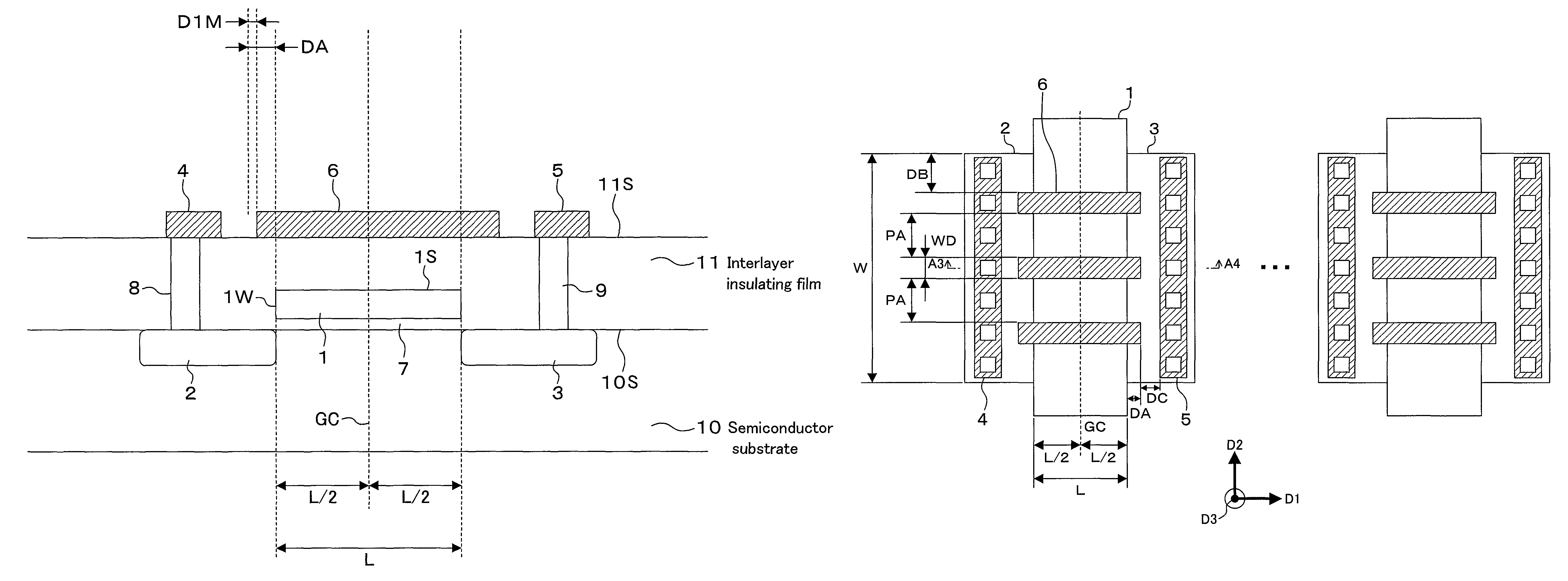
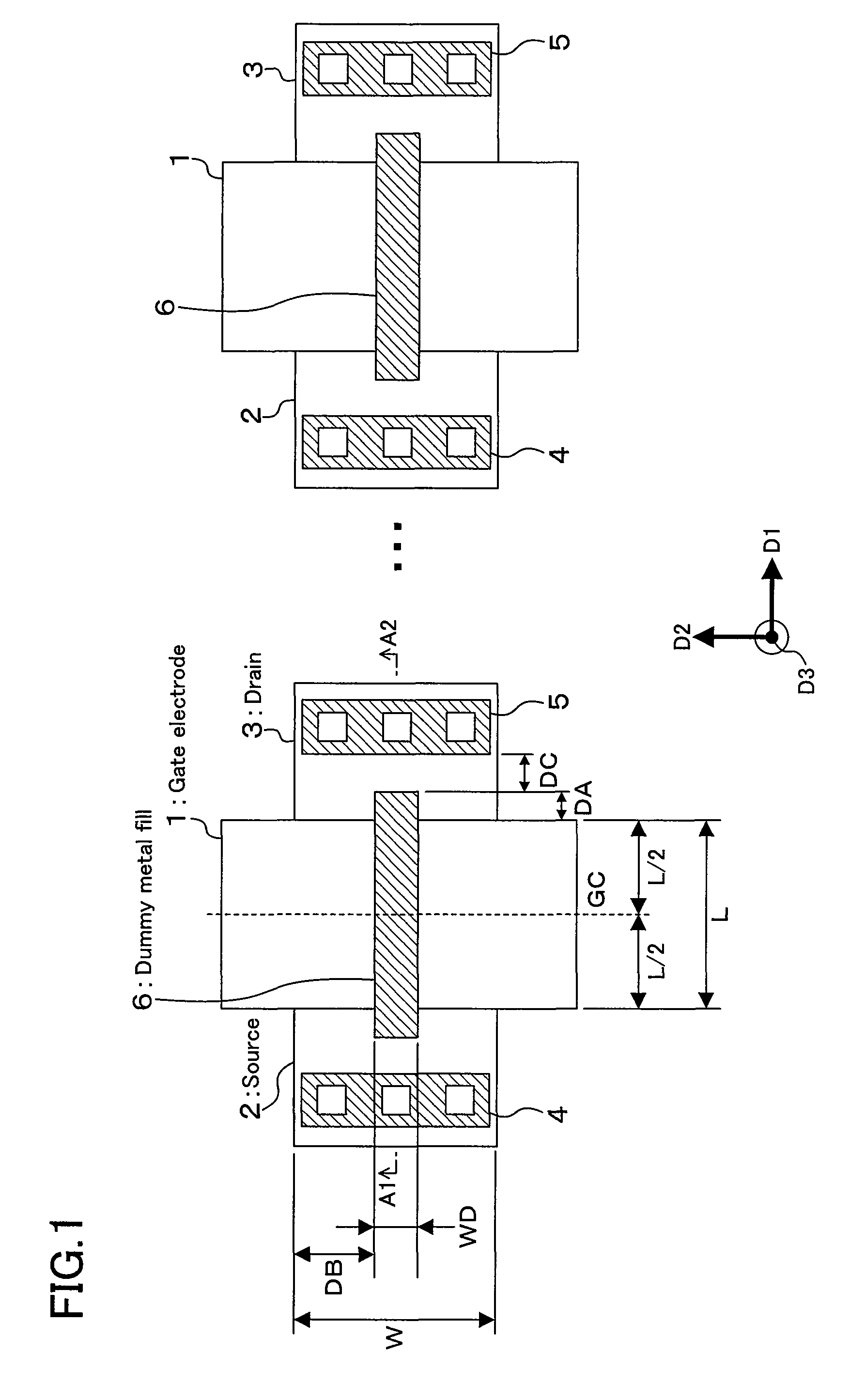
[0075]FIG. 1 is a plan view illustrating a plurality of MOS transistors (MOSFETs) formed in a semiconductor device according to Embodiment 1 of the present invention. FIG. 2 is a longitudinal section taken along the line A1-A2 shown in FIG. 1, illustrating the structure of any one of the plurality of MOS transistors.

[0076]As shown in FIGS. 1 and 2, each of the MOS transistors formed on a semiconductor substrate 10 includes a first main electrode region 2 and a second main electrode region 3 as a source and a drain (hereinafter may be referred simply to the source 2 and the drain 3), and a gate electrode 1 for controlling a current flowing between the source and the drain. The first and second main electrode regions 2 and 3 are formed within the semiconductor substrate 10. The gate electrode 1 is formed on a top surface of a gate insulating film 7 formed on part of a principle surface 10S of the semiconductor substrate 10 located between the first and second main electrode regions 2 ...

embodiment 2

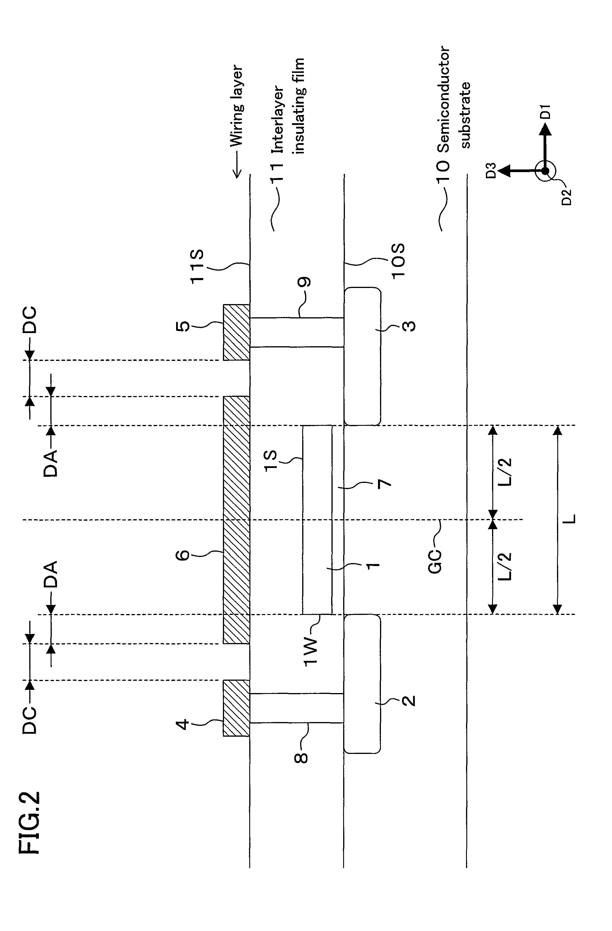
[0087]Embodiment 2 of the present invention is directed to a modified version of the semiconductor device of Embodiment 1 described above. FIG. 5 is a plan view illustrating a plurality of MOS transistors in a semiconductor device according to the present embodiment. In FIG. 5, the same components as those shown in FIG. 1 are indicated by the same reference numerals. A longitudinal section taken along the line A3-A4 indicated in FIG. 5 is the same as the longitudinal section of FIG. 2.

[0088]According to the present embodiment, as shown in FIG. 5, a plurality of dummy metal fills 6, each of which has the protrusion length DA as explained in Embodiment 1, are arranged in the second direction D2, i.e., the gate width direction, in a stripe pattern above the gate electrode 1. For example, when the channel width of the MOS transistor is greater than the maximum wiring width allowable under the design rule, the plurality of dummy metal fills 6 are arranged in a stripe pattern as shown in ...

embodiment 3

[0091]Embodiment 3 of the present invention is directed to a modified version of the semiconductor device of Embodiment 1 described above. FIG. 7 is a plan view illustrating MOS transistors in a semiconductor device according to the present embodiment. In FIG. 7, the same components as those shown in FIG. 1 are indicated by the same reference numerals. FIG. 8 is a longitudinal section taken along the line A5-A6 shown in FIG. 7. FIG. 9 is a longitudinal section taken along the line A7-A8 shown in FIG. 7.

[0092]According to the present embodiment shown in FIGS. 7 to 9, for the purpose of further size reduction of the MOS transistor of Embodiment 1, the dummy metal fill 6 is configured to overlap with the source electrode 4 as a first metal electrode and the drain electrode 5 as a second metal electrode in the first direction D1, i.e., in the gate length direction. More specifically, the source contact 8 and the drain contact 9 are arranged to have a minimum distance DD allowable under ...


PUM


Abstract

The present invention proposes a dummy metal fill structure which makes it possible to reduce variations in transistor characteristics as much as possible even if mask misalignment occurs, as well as to ensure the intended planarizing effect of the metal CMP process. The dummy metal fill formed above the gate electrode extends in the gate length direction with both ends thereof protruding from a region corresponding to the gate electrode. Even if a mask for forming a wiring layer is misaligned and the position of the dummy metal fill is misaligned from an intended position, the shape of the dummy metal fill within a region of the gate electrode is kept symmetric with respect to the center of the gate electrode.

Description

CROSS-REFERENCE TO RELATED APPLICATION[0001]This non-provisional application claims priority under 35 U.S.C. §119(a) of Japanese Patent Applications No. 2007-276325 filed in Japan on Oct. 14, 2007 and No. 2008-000339 filed in Japan on Jan. 7, 2008, the entire contents of which are hereby incorporated by reference.BACKGROUND OF THE INVENTION[0002]1. Field of the Invention[0003]The present invention relates to semiconductor devices. In particular, it relates to a technology for forming a dummy fill used for metal CMP (chemical mechanical polishing).[0004]2. Description of Related Art[0005]As the design rules for semiconductor devices become finer, a metal CMP process is commonly used to planarize an interlayer insulating film in a multilayer wiring structure.[0006]In a conventional case where the metal CMP process is applied to a semiconductor device pattern in which a large density difference lies between high density parts and low density parts, excessive polish is likely to occur i...

Claims


Application Information

Patent Timeline
Patent Type & Authority Patents(United States)
IPC IPC(8): H01L23/48
CPCH01L23/522H01L21/7684H01L2924/0002H01L2924/00
Inventor KIYOTA, AKIO
Owner PANASONIC SEMICON SOLUTIONS CO LTD
Why Eureka
Try Eureka