

Method of forming conductive lines and similar features
A conductive wire, electrical contact technology, applied in electroforming, circuits, circuit covers, etc., can solve the problems of increasing the risk of damage, expensive photoresist, reducing the overall efficiency of the device, etc., to reduce process steps and cause damage. the effect of reducing the likelihood of
- Summary
- Abstract
- Description
- Claims
- Application Information
AI Technical Summary
Problems solved by technology
Method used
Image

Examples
Embodiment Construction
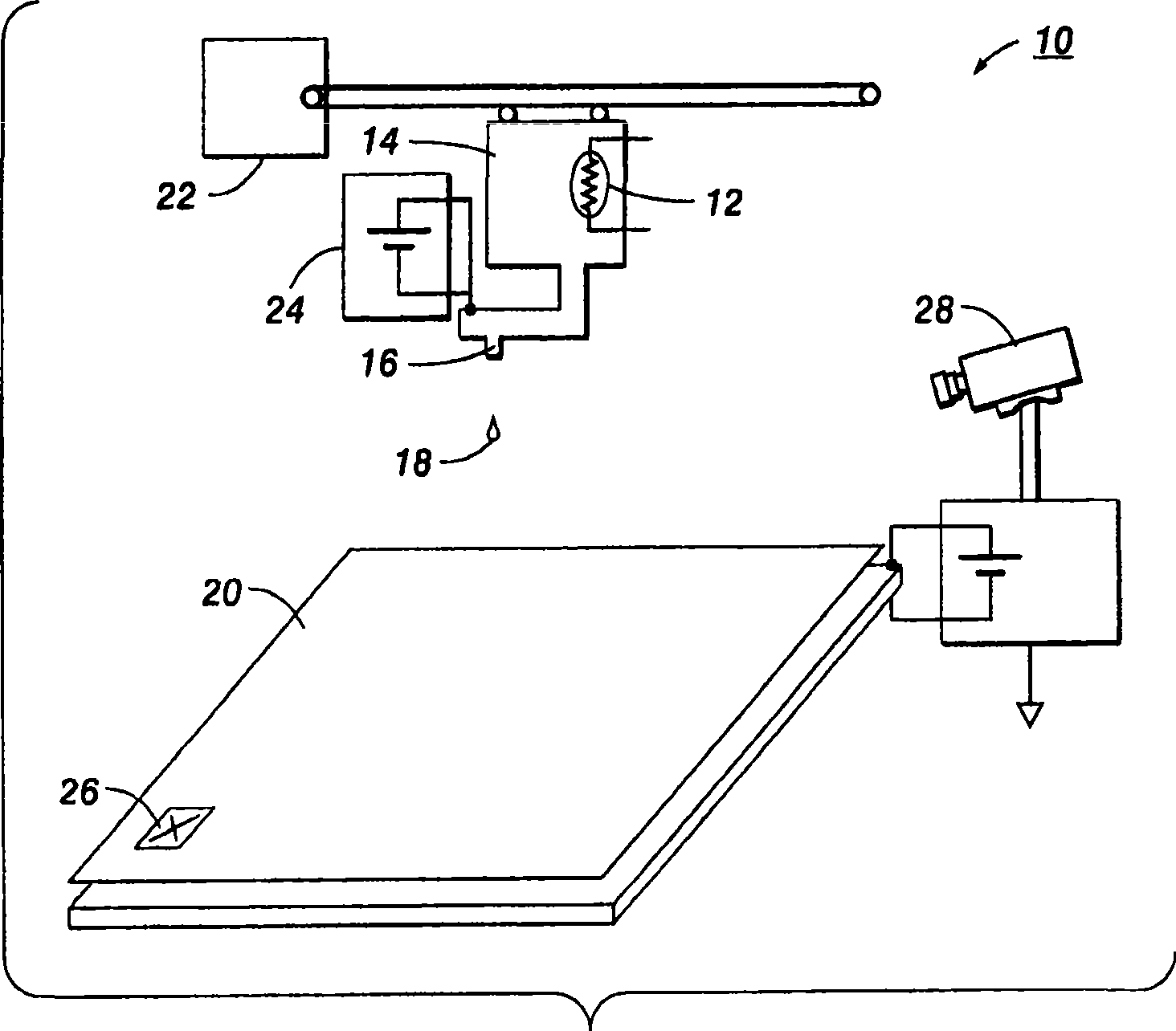
[0023] In the detailed description that follows, a method of using a print patterned mask to form conductive lines and similar features on a substrate such as might be used in a solar cell will be described. The method may use a system for generating patterns as described below, which typically uses a printer to controllably eject individual droplets to form a patterned protective layer or coating on multiple areas of the substrate to define The outline of a feature. Of course, it will be understood that other printing systems may also be used. Deposition (or removal) of material used to form various features occurs in those areas that were not once covered by the protective layer. Hence, the feature size will not be limited by the droplet size, but by how closely the droplets can be located together without combining into a single droplet.
[0024] A system suitable for practicing embodiments of the method presented herein is described in US Patent No. 6,972,261 to Wong et ...
PUM
 Abstract
Description
Claims
Application Information