Led light source unit
An LED light source and light emitting diode technology, applied in the field of light emitting diode light source units, can solve the problems of increasing the thickness of the substrate, unable to bend the LED mounting part arbitrarily, and unable to use it, so as to reduce the temperature rise of the LED, suppress the low luminous efficiency, and prevent the LED the effect of damage
- Summary
- Abstract
- Description
- Claims
- Application Information
AI Technical Summary
Problems solved by technology
Method used
Image
Examples
Embodiment 1
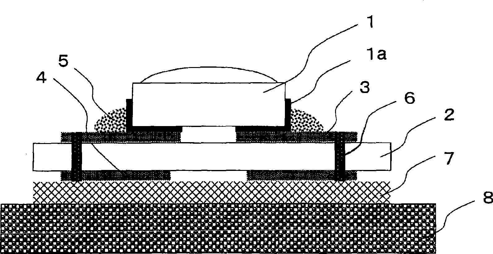
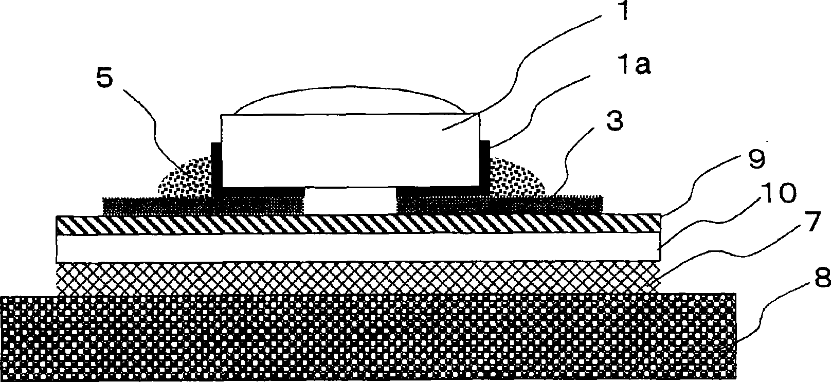
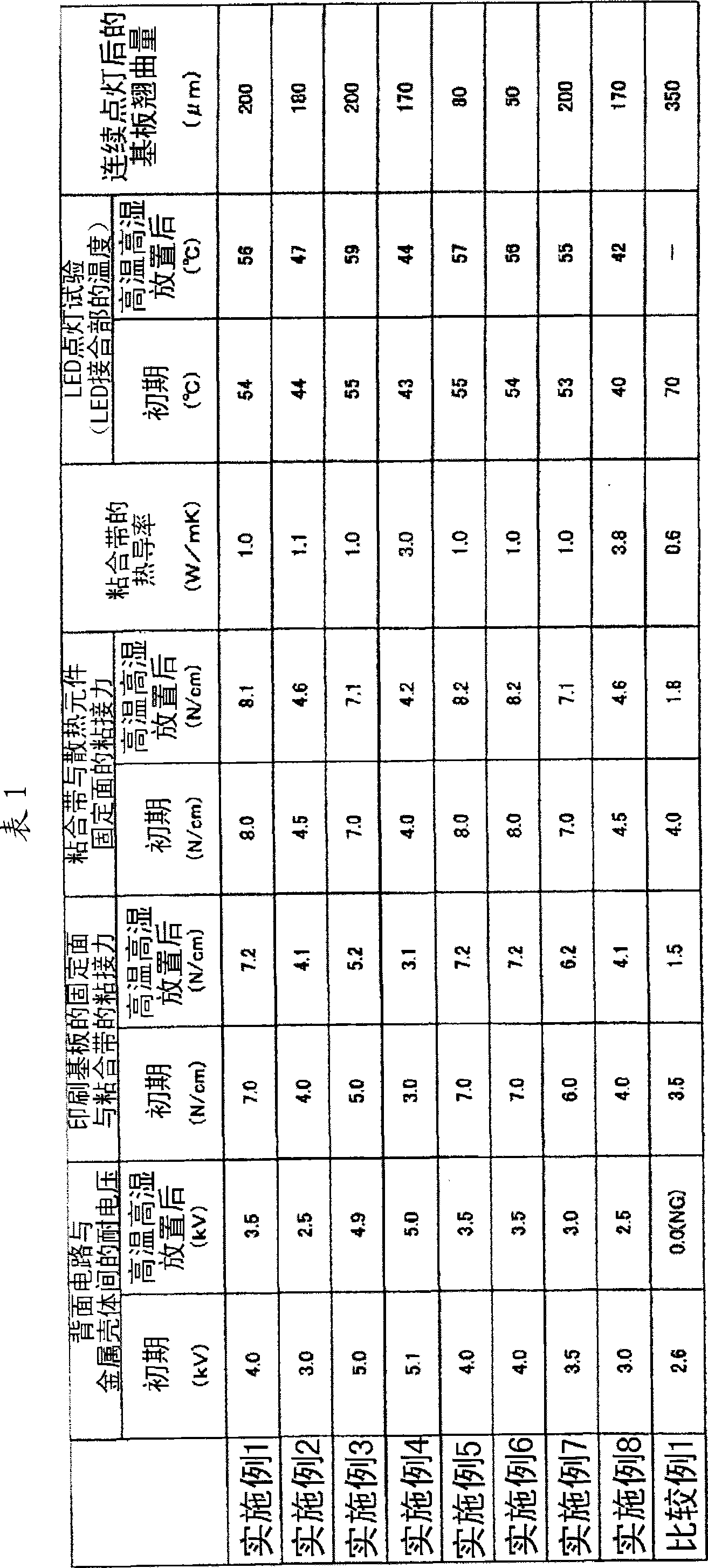
[0101] made figure 1 LED light source unit of the type shown. That is to say, for a printed circuit board with glass cloth in which 35 μm thick copper foil is formed on both sides of a 100 μm thick epoxy resin cloth impregnated with a glass substrate, at a predetermined position (the conductor connected to the electrode terminal 1a of the LED) The position where the circuit is connected to the back conductor circuit located below it) forms a via hole, and after copper plating, forms a conductor circuit for mounting LEDs, and a back conductor circuit for lighting and heat dissipation of the LED, and makes a printed circuit board.
[0102] 10% by mass of acrylic acid ( Toagosei Co., Ltd., "AA"), 0.5% by mass of photopolymerization initiator 2,2-dimethoxyl,2-diphenylethan-1-one (Seba special Chemical Co., Ltd.), 0.2% by mass of triethylene glycol dithiol (manufactured by Maruzen Chemical Co., Ltd.), and 0.2% by mass of 2-butyl-2-ethyl-1,3-propanediol diacrylate (by Kyoeisha Che...
Embodiment 2
[0129] An LED light source unit was fabricated in the same manner as in Example 1 except for the following points. That is, as the inorganic filler, alumina ("DAW-10", manufactured by Denki Kagaku Kogyo Co., Ltd.) was classified with a 45 μm sieve, and inorganic filler A having a maximum particle size of 45 μm or less and an average particle size of 9 μm was used. Then, 40 volume % of the inorganic filler A, 45 volume % of the resin composition A, and 15 volume % of the resin composition B were mixed and mixed, and the resin composition D was obtained.
[0130] Then, the resin composition D that has been subjected to defoaming treatment is coated on a PET film with a surface of 75 μm in thickness, and the PET film with a release treatment on the surface is further covered. 3000mJ / cm 2 UV rays with a wavelength of 365nm are irradiated. Thereafter, the resin composition D was cured by heat-processing at 100° C. for 3 hours to obtain an electrically insulating and heat-conducti...
Embodiment 3
[0134] An LED light source unit was fabricated in the same manner as in Example 1 except for the following points.
[0135] That is, using the same resin composition D as that used in Example 2, the resin composition D after the defoaming treatment was applied to a thickness of 46 μm on a PET film with a surface thickness of 75 μm and subjected to a release treatment, and A glass cloth with a thickness of 50 μm was laminated on the upper layer, and a PET film whose surface was subjected to a mold release treatment was further covered thereon, and the resin composition D was impregnated in the glass cloth by lamination.
[0136] Then, from the front and back at 3000mJ / cm 2 UV rays with a wavelength of 365nm are irradiated. Thereafter, the resin composition D was cured by heat-processing at 100° C. for 3 hours to obtain an electrically insulating and heat-conductive adhesive tape with a thickness of 150 μm.
[0137] Then, a solder paste (manufactured by Senju Metal Co., Ltd., ...
PUM
 Abstract
Description
Claims
Application Information


