

Wafer quality analysis apparatus and method
A quality analysis device and quality analysis technology, applied in the direction of comprehensive factory control, instrumentation, comprehensive factory control, etc., can solve the problems of missing wafer process and incomplete analysis of wafer quality analysis methods, and achieve the effect of improving accuracy
- Summary
- Abstract
- Description
- Claims
- Application Information
AI Technical Summary
Problems solved by technology
Method used
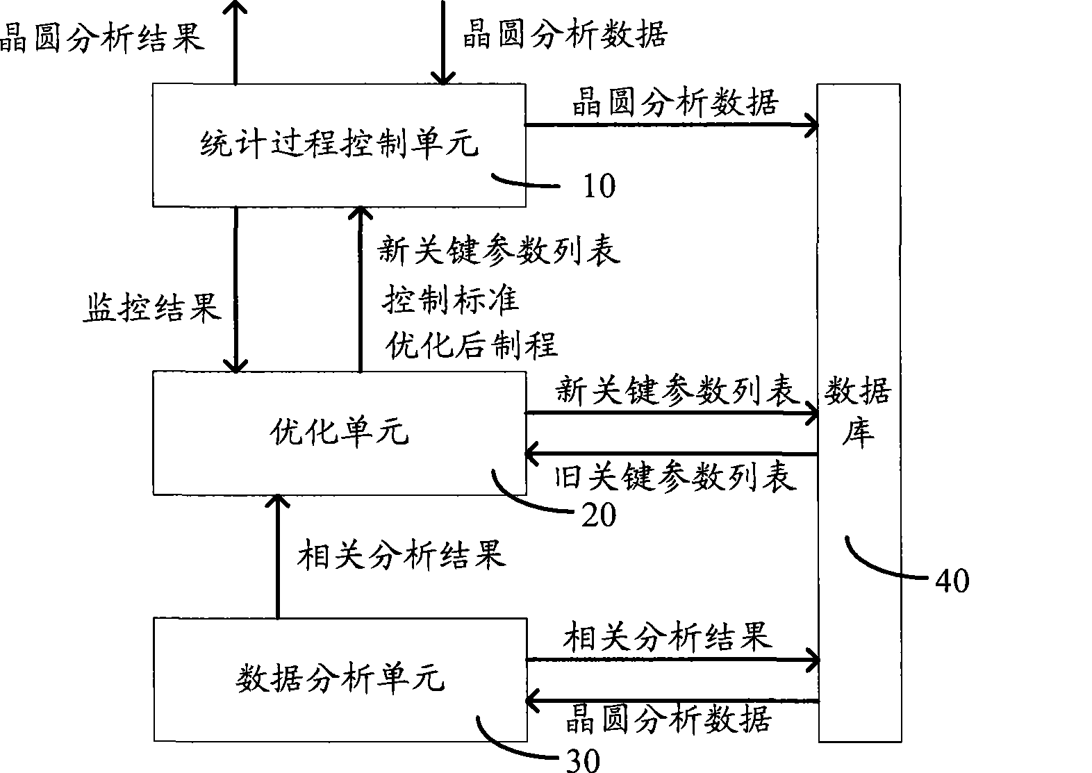
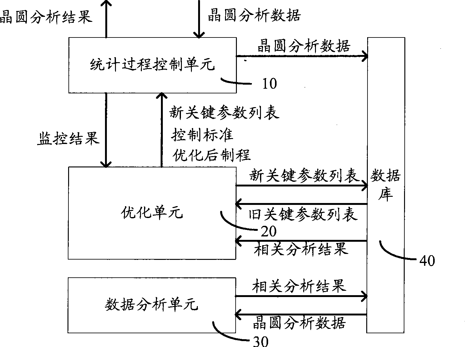
Image

Examples
Embodiment approach
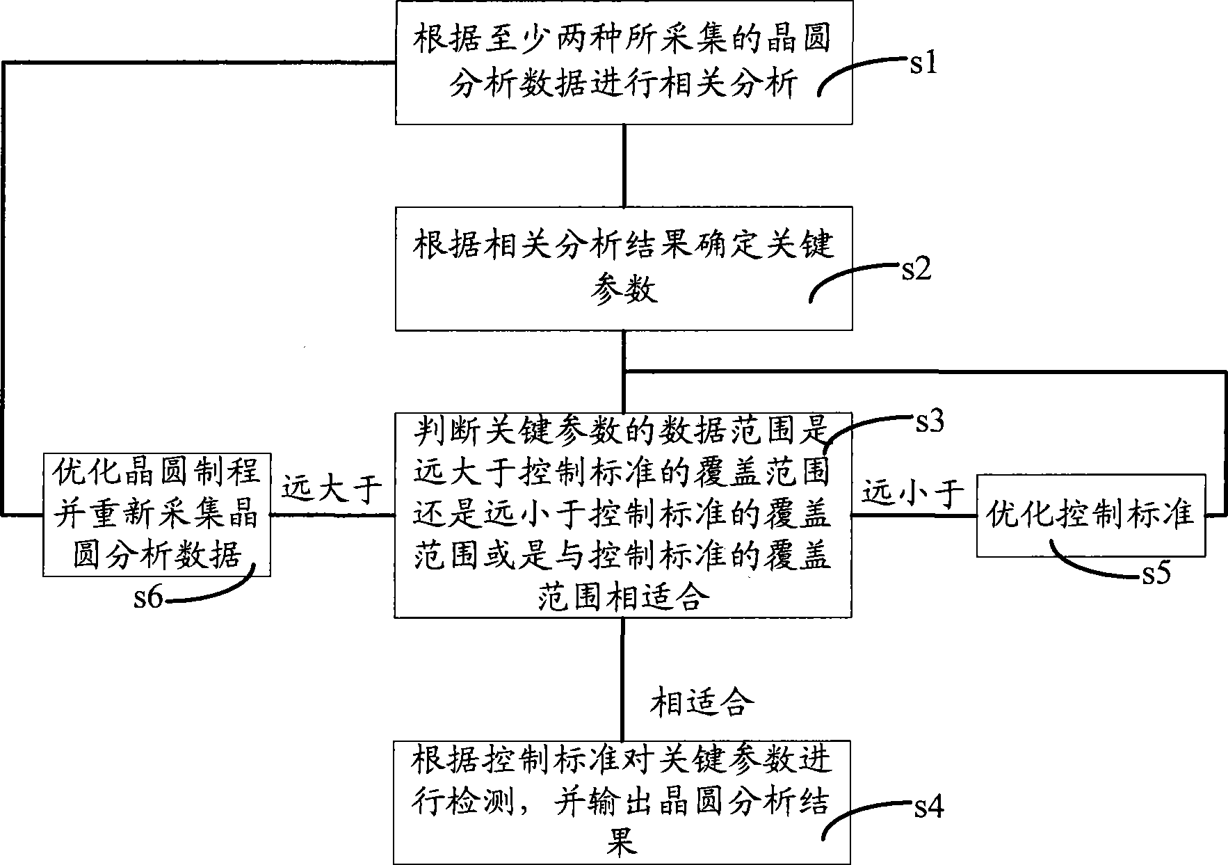
[0039] refer to figure 1 As shown, an embodiment of the wafer quality analysis method of the present invention comprises the following steps,
[0040] Step s1, performing correlation analysis according to at least two types of collected wafer analysis data;
[0041] Step s2, determining key parameters according to relevant analysis results;
[0042] Step s3, judging whether the data range of key parameters is much larger than the coverage range of the control standard, far smaller than the coverage range of the control standard or suitable for the coverage range of the control standard, if the data range of the key parameter is suitable for the coverage range of the control standard, Then execute step s4; if the data range of the key parameter is much smaller than the coverage of the control standard, then execute step s5; if the data range of the key parameter is far beyond the coverage of the control standard, then execute step s6;
PUM
 Abstract
Description
Claims
Application Information