Semiconductor device

A semiconductor and component technology, applied in the field of semiconductor devices, can solve the problems of increasing the number of parts of semiconductor devices and complicated parts handling, and achieve the effect of reducing inductance

Inactive Publication Date: 2009-06-24
HONDA MOTOR CO LTD
View PDF1 Cites 21 Cited by
  • Summary
  • Abstract
  • Description
  • Claims
  • Application Information

AI Technical Summary

Problems solved by technology

Therefore, when manufacturing the converter device, there is a problem that the number of parts forming the semiconductor device increases, and the handling of the parts is also troublesome for the manufacturer.

Method used


Image

  • Semiconductor device
  • Semiconductor device
  • Semiconductor device

Examples


Embodiment 1

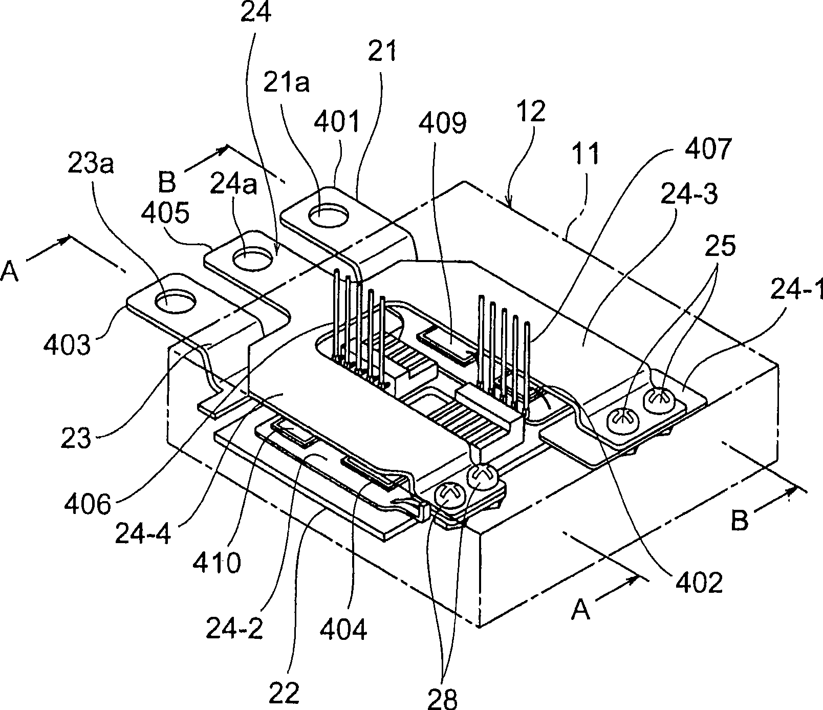
[0062] refer to Figure 1 to Figure 5 A first embodiment of the semiconductor device of the present invention will be described.

[0063] The semiconductor device described in this embodiment is a power semiconductor device, which is represented as a converter device for driving a driving three-phase motor of an electric vehicle. figure 1 The shown IGBT module represents the main part of the converter arrangement. First, refer to Figure 4 The configuration of the circuit of the IGBT module will be described.

[0064] Figure 4 Indicates a circuit portion of one phase (one of U phase, V phase, and W phase) of the bridge circuit of the converter device. Figure 4 The illustrated circuit includes a high-voltage side IGBT element 402 arranged on the side of a high-voltage terminal 401 and a low-side IGBT element 404 arranged on the side of a low-voltage terminal 403 . In addition, the semiconductor element used in the semiconductor device of this embodiment is not limited to...

Embodiment 2

[0104] Below, refer to Figure 6 ~ Figure 9 A second embodiment of the semiconductor device of the present invention will be described.

[0105] Like the first embodiment, the semiconductor device of the second embodiment is an electric power semiconductor device, typically a converter device for driving a driving three-phase motor of an electric vehicle. Figure 6 is the same as above figure 1 same graph.

[0106] For the structure of the circuit of the IGBT module of the second embodiment, there is Figure 4 structure as described.

[0107] That is, in the circuit portion of one phase (one of the U phase, V phase, and W phase) of the bridge circuit of the converter device, the high-voltage side IGBT element 402 disposed on the high-voltage terminal 401 side and the high-voltage side IGBT element 402 disposed on the low-voltage terminal side are included. The low side IGBT element 404 on the 403 side. The bridge circuit of the converter device is composed of six power se...

Embodiment 3

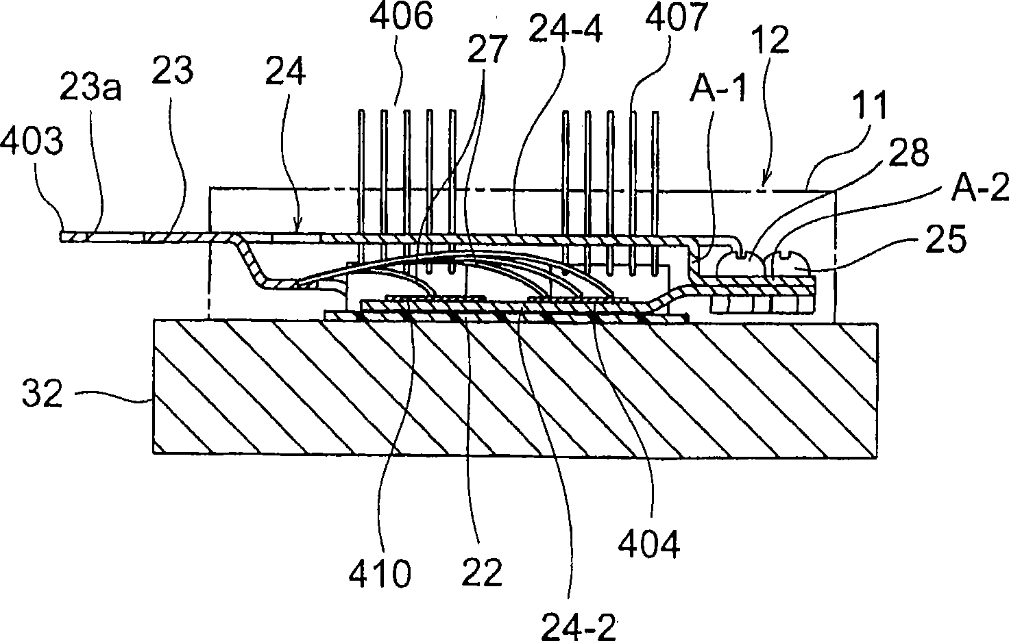
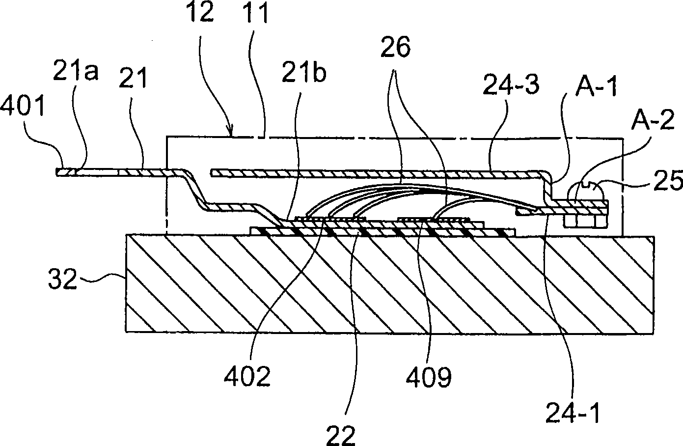
[0142] refer to Figure 11 ~ Figure 13 , an example of the basic structure of the semiconductor device according to the third embodiment of the present invention will be described. The semiconductor device of the third embodiment is also used in a converter device for driving a driving three-phase motor of an electric vehicle, as in the above-mentioned embodiments.

[0143] refer to Figure 11 ~ Figure 13 Describe the physical structure of the IGBT module.

[0144] exist Figure 11 and Figure 12 In , the block part 211 indicated by the two-dot chain line shows the appearance shape of the package forming the IGBT module 212 . The block member 211 is actually a molded part made of resin. Figure 11 The portion indicated by the solid line in the center is a physical structural portion of the wiring board. In addition, resin molding 211 in Figure 11 and Figure 12 represented by imaginary lines in Figure 13 is represented by a solid line.

[0145] exist Figure 11 Amon...


PUM


Abstract

A semiconductor device is composed of a pair of semiconductor chips (402, 404) arranged parallel on the same flat plane; a high voltage bus bar (21) bonded on the surface on the collector side of one semiconductor chip (402); a low voltage bus bar (23) connected to the surface on the emitter side of the other semiconductor chip (404) with a bonding wire (27); a first metal wiring board (24-1) connected to the surface on the emitter side of the semiconductor chip (402) with a bonding wire (26); a second metal wiring board (24-2) bonded on the surface on the collector side of the semiconductor chip (404); a third metal wiring board (24-3) connected to the first metal wiring board (24-1); a fourth metal wiring board (24-4) connected by being bent from an end portion of the second metal wiring board (24-2); and an output bus bar (24) having output terminals (405) extending from each end portion of the third metal wiring board (24-3) and that of the fourth metal wiring board (24-4).

Description

technical field [0001] The present invention relates to a semiconductor device, and more particularly to a semiconductor device for electric power including an IGBT module used in a drive circuit for driving a drive motor of an electric vehicle. Background technique [0002] In an electric vehicle such as an electric automobile, a converter device for driving a driving motor thereof is used. The converter device includes a circuit connecting the conversion elements through a bridge circuit structure. The converter device switches the current flowing in the drive motor by appropriately turning on / off the switching elements of the bridge circuit. As conversion elements (power semiconductor elements) constituting the bridge circuit, power transistors, IGBTs, FETs, IEGTs, and the like are widely used. The converter device generally has a module structure in which a plurality of conversion elements are housed in one package. [0003] When the driving motor of an electric vehic...

Claims


Application Information

Patent Timeline
Patent Type & Authority Applications(China)
IPC IPC(8): H01L25/07H01L25/18
CPCY02T10/7241H01L2224/49113H01L2224/48091H01L2224/48247H01L2924/30107H01L2924/13055H01L2924/13091H01L2224/49111H01L2924/181H01L2924/00014H01L2924/00H01L2924/00012
Inventor 高野文朋渡边信也合叶司大塚浩中岛穰二
Owner HONDA MOTOR CO LTD
Why Eureka
Try Eureka