Waveguide interface

A waveguide interface, waveguide technology, applied in waveguide-type devices, circuits, electrical components, etc.

Inactive Publication Date: 2009-07-15
HARRIS STRATEX NETWORKS OPERATING
View PDF0 Cites 17 Cited by
  • Summary
  • Abstract
  • Description
  • Claims
  • Application Information

AI Technical Summary

Problems solved by technology

This characteristic is optimized for the entire frequency band

Method used


Image

  • Waveguide interface
  • Waveguide interface
  • Waveguide interface

Examples


Embodiment Construction

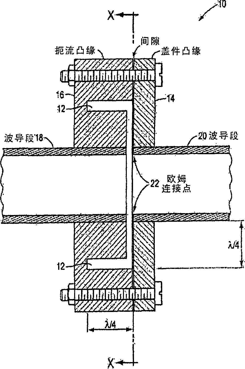
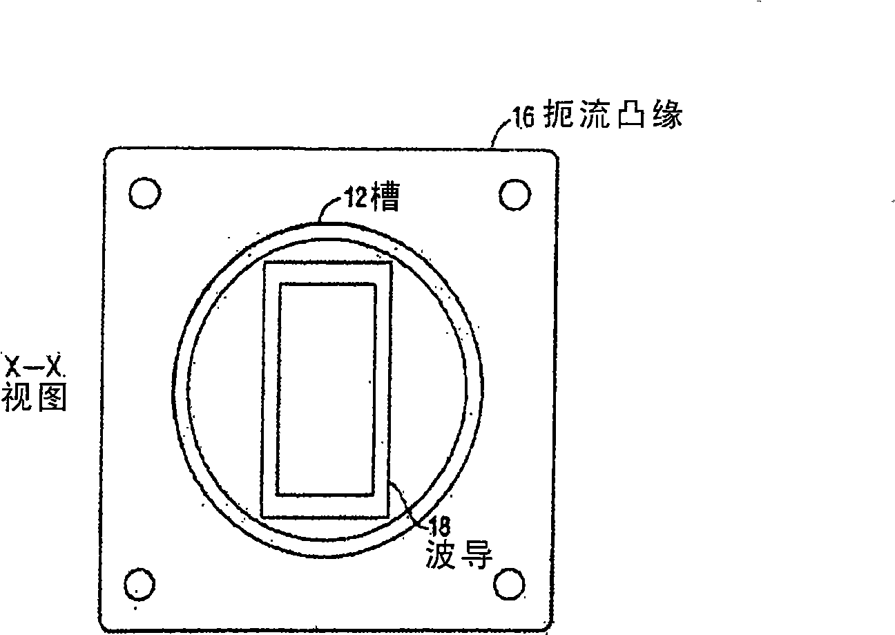
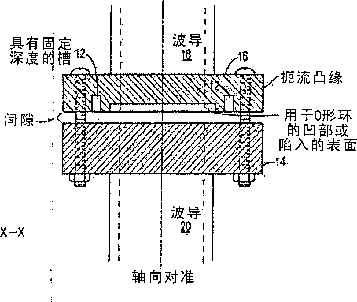
[0023] As noted above, the present invention relates to waveguide interfaces. The design of the waveguide interface according to the invention is partly based on the realization that with suitable geometry, a half-wave slot at the connection point between two waveguides presents for passing waves a virtual continuity through the transmission line joint.

[0024] Figure 4a The above principle is illustrated. The transmission line is interrupted by a slot 302 having a half wavelength dimension (λ / 2). The tank is similar to a tank circuit with an inductance L and a capacitance C. The resonant frequency fc of this similar tank circuit is given by:

[0025] 1. fc = 1 2 π LC

[0026] The resonance frequency fc is the center frequency of the frequency band. Figure 4b The graph of shows that the resonant frequency of the tank circuit is in the frequency b...


PUM


Abstract

The present invention relates to a waveguide interface. Waveguide flanges for joining waveguide sections or components are designed to achieve mechanical strength and exhibit desired electrical properties such as low insertion loss and high return loss. The present invention contemplates waveguide interfaces with a choke flange designed to engage with a shield flange and provide a joint with improved electrical properties. The new choke designs produce a virtual continuity through the waveguide joints and minimize electrical energy leakage. The electrical and mechanical properties of the joint in the waveguide interfaces are robust and able to tolerate lower levels of parts precision, imperfect mating of the flanges without metal-to-metal contact and gaps up to 0.06'' or more between the mating flange surfaces.

Description

technical field [0001] The present invention relates to waveguide systems, and more particularly to waveguide interfaces for coupling multi-section waveguides and waveguide elements. Background technique [0002] Waveguide flanges are used to couple waveguide segments and waveguide elements. When designing waveguide flanges for waveguide splices, consideration is given to the fact that the characteristics of the waveguide splice affect the mechanical strength and electrical performance of the waveguide. Therefore, waveguide joints are designed to provide strength and minimize energy reflections and power leakage across the frequency range. [0003] Ideally, flat flanges abutting together with perfect ohmic contact would produce frequency insensitive, negligible reflections and power leakage. With perfect contact coupling of the flat flanges, the waveguide passes substantially continuously through the joint. However, preventing leaks and reflections with perfect ohmic cont...

Claims


Application Information

Patent Timeline
Patent Type & Authority Applications(China)
IPC IPC(8): H01P1/04
CPCH01P1/042
Inventor 茵-芳·朝布鲁斯·库凯尔埃里克·同森约翰·鲁伊滋
Owner HARRIS STRATEX NETWORKS OPERATING
Why Eureka
Try Eureka