Waveguide thermo-optic switch and manufacturing method thereof

A manufacturing method and technology of optical switches, applied in optics, nonlinear optics, instruments, etc., can solve the problems of low reliability, large insertion loss, poor stability, etc., and achieve improved performance indicators, low driving power, and reduced production costs. Effect

Inactive Publication Date: 2016-07-13
苏州峰通光电有限公司
View PDF3 Cites 9 Cited by
  • Summary
  • Abstract
  • Description
  • Claims
  • Application Information

AI Technical Summary

Problems solved by technology

[0004] For this reason, the technical problem to be solved by the present invention is that the thermo-optic switch with the existing organic/inorganic hybrid structure has a large in

Method used


Image

  • Waveguide thermo-optic switch and manufacturing method thereof
  • Waveguide thermo-optic switch and manufacturing method thereof
  • Waveguide thermo-optic switch and manufacturing method thereof

Examples


Embodiment 1

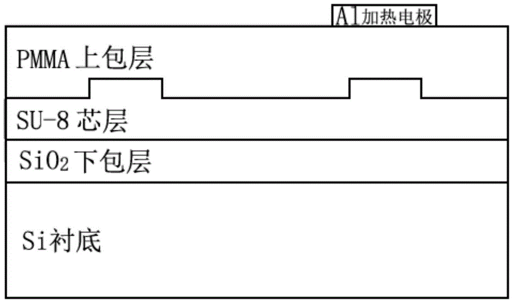
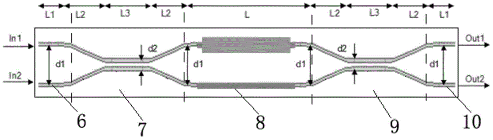
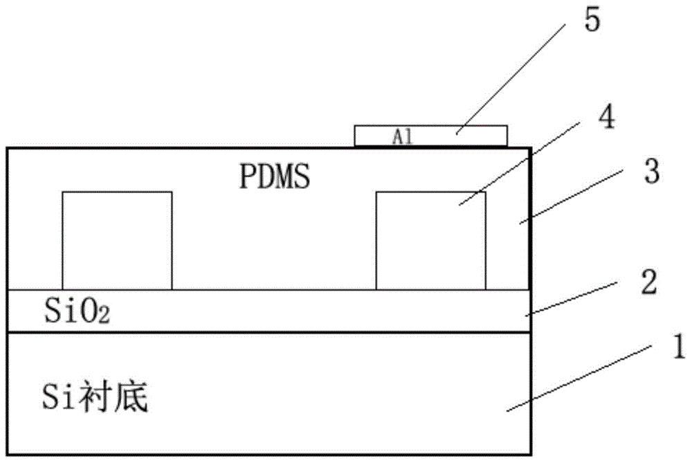
[0046] Such as figure 2 and 3As shown, this embodiment provides a waveguide thermo-optic switch, which sequentially includes a substrate 1, a lower cladding layer 2, an upper cladding layer 3 and a heating electrode 5, and the lower cladding layer 2 is SiO 2 Materials, the upper cladding layer 3 is a polymer material, which is sequentially divided into the input waveguide area 6, the first beam splitting and beam combining area 7, the thermo-optic modulation area 8, the second beam splitting and beam combining area along the length direction of the waveguide thermo-optic switch Region 9 and output waveguide region 10, between the lower cladding layer 2 and the upper cladding layer 3, there are two waveguide cores 4 penetrating in the upper cladding layer 3 along the length direction of the waveguide thermo-optic switch, and the waveguide of the thermo-optic modulation region 8 The material of the core 4 is polymer, and the material of the waveguide core 4 in other regions is...

Embodiment 2

[0057] This embodiment provides a method for manufacturing a waveguide thermo-optical switch, including the following steps:

[0058] In the first step, the lower cladding layer 2 is fabricated on the substrate 1, and the material of the lower cladding layer is SiO 2 . Specifically, firstly, a layer of SiO with a thickness of 3 μm is grown on the substrate 1 of Si material by plasma enhanced chemical vapor deposition (PECVD). 2 material layer, followed by high temperature annealing. The specific process of high temperature annealing is: firstly, the temperature is raised to 120°C at a heating rate of 10-20°C / min and kept for 20-30min; then the temperature is raised to 140°C at a heating rate of 10-20°C / min and kept for 20-30min; Then, raise the temperature to 160°C at a heating rate of 10-20°C / min and keep it warm for 20-30min; finally, cool to room temperature with the furnace. Through the above-mentioned annealing and hardening method, lattice defects and internal stress ...


PUM

PropertyMeasurementUnit
Heightaaaaaaaaaa
Lengthaaaaaaaaaa
Widthaaaaaaaaaa

Abstract

The invention relates to a waveguide thermo-optic switch and a manufacturing method thereof. The waveguide thermo-optic switch sequentially comprises a substrate, a lower cladding, an upper cladding and a heating electrode, wherein the lower cladding is made from an SiO2 material, and the upper cladding is made from a polymer material; the waveguide thermo-optic switch is sequentially divided into an input waveguide area, a first beam splitting and combining area, a thermo-optic modulation area, a second beam splitting and combining area and an output waveguide area along the length direction; two waveguide cores arranged in the upper cladding in a penetrating way along the length direction of the waveguide thermo-optic switch are positioned between the lower cladding and the upper cladding; the waveguide cores in the thermo-optic modulation area are made from the polymer material, and the waveguide cores in the other areas are made from a doped SiO2 material. The technical problems that the existing thermo-optic switch having an organic/inorganic hybrid structure is high in insertion loss, low in reliability and poor in stability can be solved. Furthermore, a subsequent encapsulation process of the waveguide thermo-optic switch is also compatible with the existing mainstream encapsulation process, so that additional input is not increased.

Description

technical field [0001] The invention relates to the technical field of semiconductors. Specifically, it relates to a waveguide thermo-optic switch and a manufacturing method thereof. Background technique [0002] Compared with existing optical switches such as mechanical optical switches, liquid crystal optical switches, and MEMS optical switches, waveguide optical switches have obvious advantages in reliability because they have no mechanical moving parts. Among waveguide optical switches, thermo-optical switches have the advantages of small size, simple process, and good stability. Waveguide thermo-optical switches have broad development prospects in the fields of optical communication, optical computing, and optical sensing. They have important applications in protecting communication networks, detecting communication networks, and detecting optical devices, especially in optical communication systems. Switches are an important part of optical add-drop multiplexers and ...

Claims


Application Information

Patent Timeline
IPC IPC(8): G02F1/01
CPCG02F1/011G02F1/0147G02F2202/022G02F2202/06
Inventor 田亮髙任峰汪昌君马春雷
Owner 苏州峰通光电有限公司
Why Eureka
Try Eureka