Switching power supply

A technology of switching power supply and high-side switch, which is applied in the direction of electrical components, high-efficiency power electronic conversion, output power conversion devices, etc., can solve the problems of discontinuous input current waveform, no miniaturization and low energy conduction efficiency, and achieve Effects of reduced driving power, improved parts count, and improved reduction

Inactive Publication Date: 2009-03-18
HITACHI LTD
View PDF1 Cites 13 Cited by
  • Summary
  • Abstract
  • Description
  • Claims
  • Application Information

AI Technical Summary

Problems solved by technology

However, since the on-off operation is always performed simultaneously regardless of the magnitude relationship between the instantaneous value of the input voltage and the voltage value of the output smoothing capacitor, the energy accumulated in the coil is transferred to the output smoothing capacitor when the switch is turned off. In the side discharge mode, the input power is always cut off, the input current becomes completely 0, and the input current waveform becomes discontinuous
Therefore, the conduction efficiency of energy from input to output is low, and as a result, in the circuit of Patent Document 1, the amount of input current per switch increases compared with a general boost circuit. Circuit efficiency is disadvantageous on the point of
The input current waveform is always discontinuous. The waveform deformation of (3) is also the reason for the deformation to become larger.
In addition, there is no description related to (2) miniaturization and thinning in the above-mentioned patent documents.

Method used


Image

  • Switching power supply
  • Switching power supply
  • Switching power supply

Examples


Embodiment 1

[0035] 1st Embodiment of this invention is demonstrated using FIG.1 and FIG.2, FIG.3, FIG.4, FIG.5.

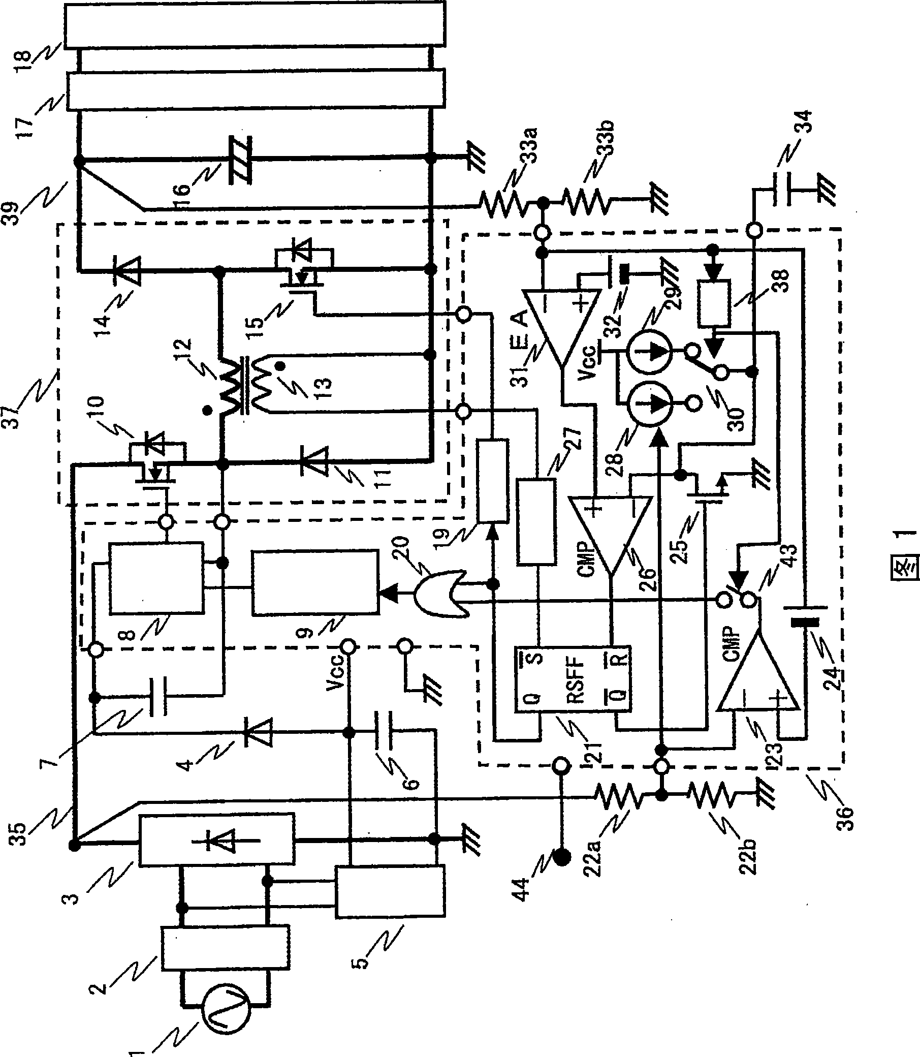
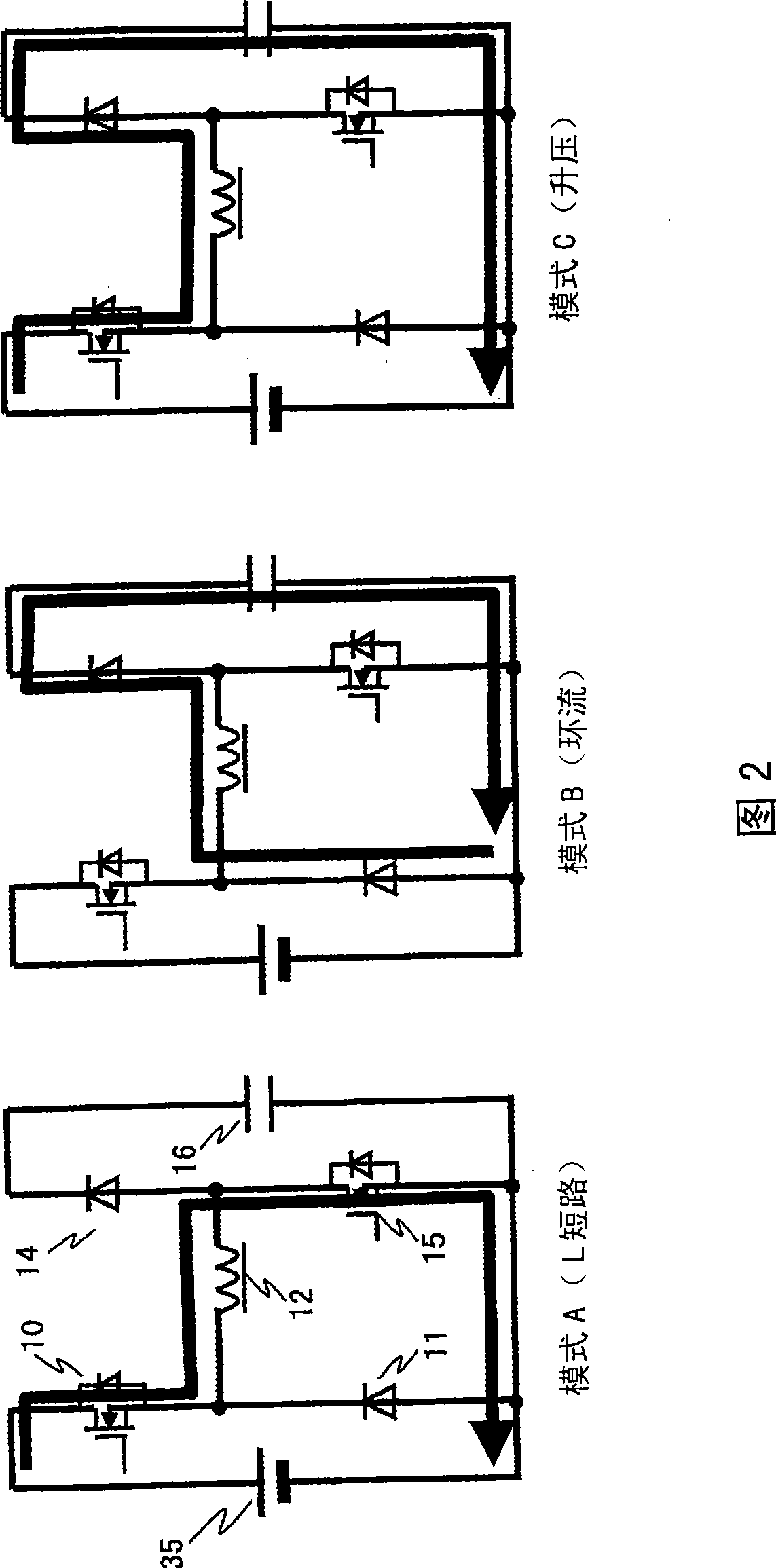
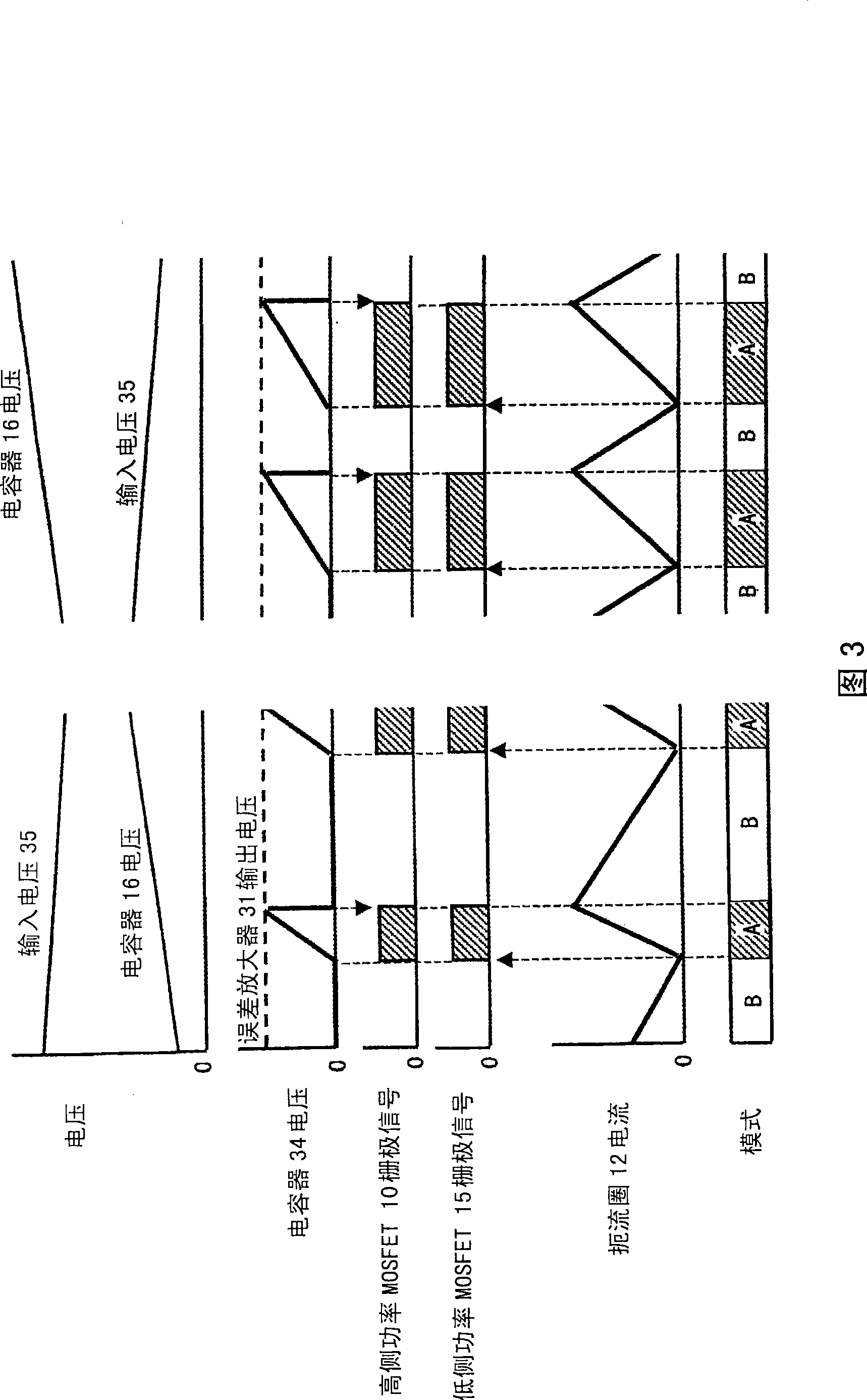
[0036] FIG. 1 is a circuit diagram showing a first embodiment of a buck-boost switching power supply of the present invention. The configuration of Fig. 1 will be described. The AC power supply 1 becomes the input voltage 35 through the input filter 2 and the rectifier 3, and becomes a full-wave rectified waveform. In addition, an auxiliary power supply 5 is connected to the input filter 2 . On the DC output side of the rectifier 3 , the voltage dividing resistors 22 a , 22 b are both connected to the drain of a high-side (side) power MOSFET 10 . One end of a choke coil (choke coil) 12 (start of winding) and a cathode of a freewheel diode 11 are connected to the source of the high-side power MOSFET 10 . The anode of the freewheeling diode 11 is connected to the ground of the rectifier 3 . Also, the drain of the low-side power MOSFET 15 and the anode of the boost diode 14 a...

Embodiment 2

[0079] Next, a second embodiment of the present invention will be described with reference to FIGS. 6 , 7 , 8 , and 9 . FIG. 6 shows the main circuit portion of the buck-boost switching power supply, and FIG. 7 shows its control circuit. In FIGS. 6 and 7 , the same reference numerals are assigned to the same components as in FIG. 1 . The difference between the main circuit section in FIG. 6 and FIG. 1 is that two sets of main circuits, ie, H-bridge circuits, are prepared and connected in parallel. That is, the connection form of the high-side power MOSFET 10a, the freewheeling diode 11a, the choke coil 12a, the low-side power MOSFET 15a, and the boost diode 14a constituting the H-bridge circuit 37 is the same as that of the main circuit of FIG. 1 . In addition, in FIG. 6 , there are high-side power MOSFET 10b, freewheel diode 11b, choke coil 12b, low-side power MOSFET 15b, and boost diode 14b, and these are also connected in the same manner. In addition, the drains of the hi...

Embodiment 3

[0091] Next, other embodiments of the present invention will be described using FIG. 10 and FIG. 11 .

[0092] Fig. 10 is the main circuit of the buck-boost switching power supply of the present invention similar to Fig. 6 and Fig. 1 . In FIG. 10 , the same reference numerals are assigned to the same components as those in FIG. 6 or FIG. 1 . Here, points different from those in FIG. 6 will be described. In FIG. 10 , the high-side power MOSFET 10 , the circulating diode 11 , the choke coil 12 a, the low-side power MOSFET 15 a, and the boost diode 14 a constituting the H-bridge circuit 37 are connected in the same way as the main circuit in FIG. 1 or FIG. 6 . In FIG. 10 , a choke coil 12 b and a choke coil 12 a are connected in parallel, and these two choke coils are connected to the source of the high-side power MOSFET 10 from FIG. 6 . In other words, the high-side power MOSFET 10b and its drive circuit system described in FIG. 6 are omitted.

[0093] Next, Fig. 11 will be d...


PUM


Abstract

The invention provides a switching power supply, and provides a buck-boost converter of an H bridge type having a function for initially charging a smoothing output capacitor without a relay and a rush current preventing resistance. In the prior art, the resistance and the relay for preventing current shock is not removed required by the switching power supply. In addition, in AC1000V, since buck-boos of the PFC converter is high, efficiency is low and fever is large, thereby blocking minitype thinning of the power supply. The PFC converter is changed into a current critical H bridge type, realizing initial charging function of the smoothing capacitor of the circuit.

Description

technical field [0001] The invention relates to a switching power supply for improving the power factor of an AC input current, Background technique [0002] In order to rectify and smooth the AC power supply to obtain DC, although the configuration using a diode bridge and a smoothing capacitor is the simplest, in this configuration, the input current flows only around the peak value of the power supply voltage, that is, a capacitor input type rectification circuit, resulting in a drop in power factor or an increase in input high-order harmonics. The problem of inputting harmonics is regulated by international standards, and countermeasures based on input power are required. For this trend, various converters called power factor improvement (PFC: PowerFact or Correction on) converters or high power factor converters have been proposed. [0003] Among them, the most common circuit is a circuit method called a PFC converter, which is a circuit composed of AC as follows: con...

Claims


Application Information

Patent Timeline
Patent Type & Authority Applications(China)
IPC IPC(8): H02M1/42H02M7/04
CPCH02M2001/007Y02B70/126H02M1/4233H02M3/1582Y02B70/10H02M1/007H02M1/0085
Inventor 叶田玲彦北村诚樱森房夫望月刚
Owner HITACHI LTD
Why Eureka
Try Eureka