

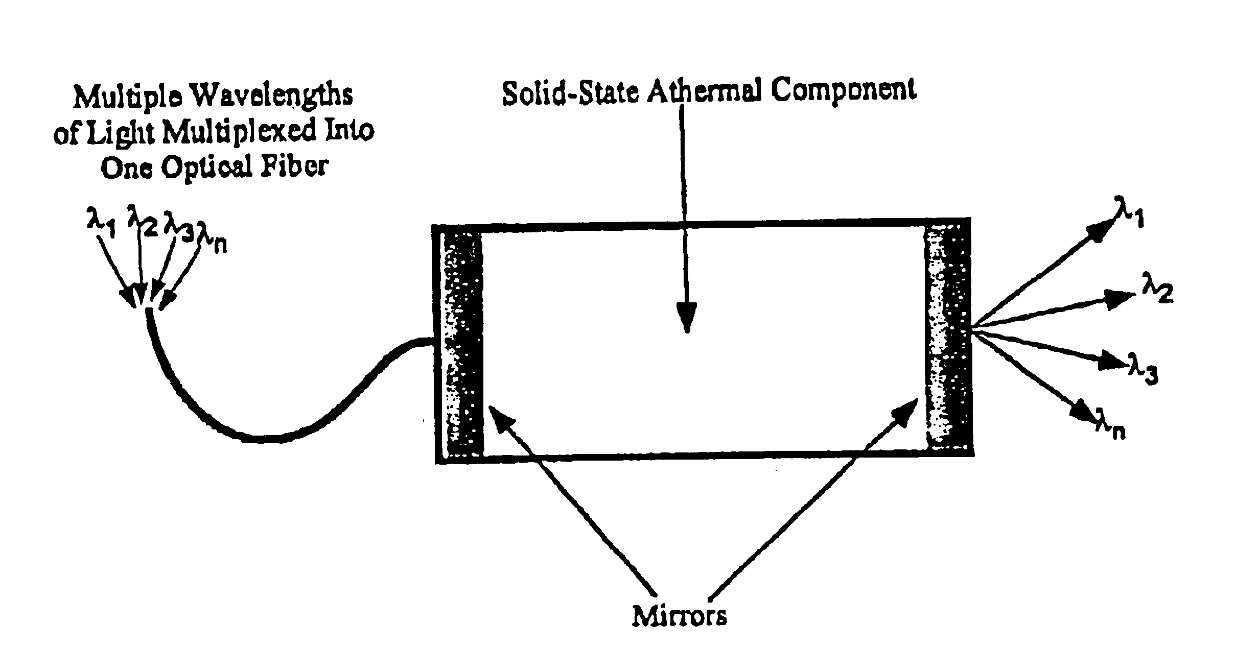
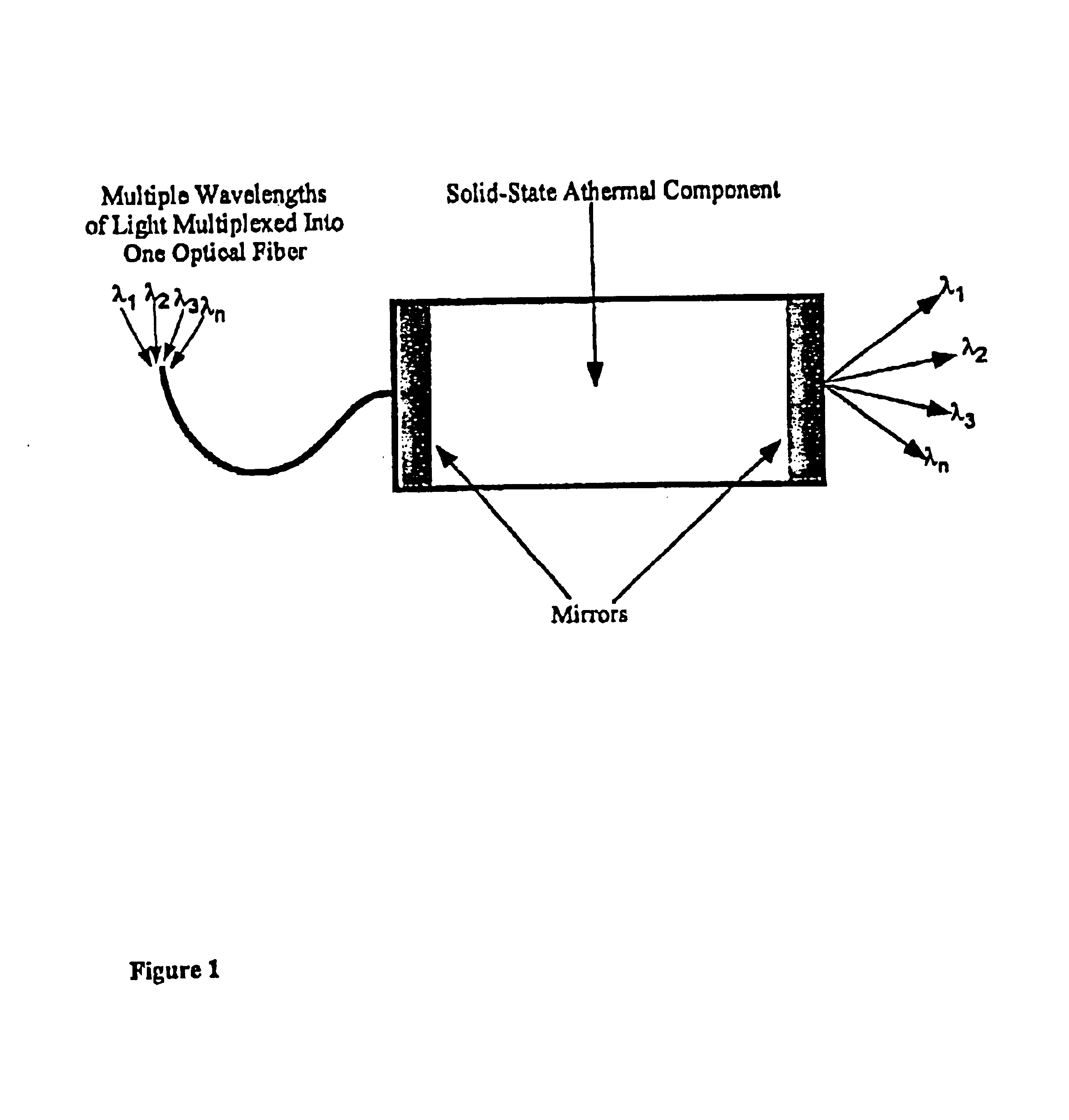
Athermal optical components
a technology of optical components and thermal insulation, applied in the field of thermal insulation optical devices, can solve the problems of only varying success of the experiment, and traditional glasses will not meet the requirements of the invention
- Summary
- Abstract
- Description
- Claims
- Application Information
AI Technical Summary
Benefits of technology
Problems solved by technology
Method used
Image

Examples
example 1
Composite Material: Glass to Polymer
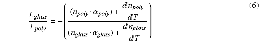
The polymer, PMMA, (see properties in Table I), is joined to an optically transparent glass, Schott BK-7 (Available from Schott Glass Technologies, Duyrea, Pa.) (see properties in Table 1), to yield a composite material that has solid state athermal properties.
The polymer layer is typically much thinner (100 to 10000 times thinner) than the glass, due to the requirement set forth by Equation (6). This thin layer of polymer is joined to the glass by any of the following techniques:1) Sputtering a thin film of PMMA onto the glass;2) Dip coating the glass in methyl methacrylate monomer, and then curing the monomer to form PMMA using heat and / or UV light;3) Joining a thin section of PMMA to the glass with a UV curing epoxy and then grinding and polishing away the excess polymer to yield the correct thickness;4) Joining a thin section of PMMA to the glass with any type of optically transparent adhesive and then grinding and polishing away the excess po...
example 2
Composite Material: Crystal to Polymer
Crystals typically have a large thermal expansion coefficient, and their optical path lengths generally increase as the temperature increases (even though a crystal may have a negative dn / dT, see Table I). Thus, a crystal is joined to a polymer (in the same way that a lass was in Example #1) to yield a solid state athermal material. The increase in optical path length of the crystal (with increasing temperature) will be offset by the decreasing optical path length of the polymer (with increasing temperature) to yield a solid state athermal material (when joined together). An equation with the same form as Equation (6) is used to calculate the thickness of the crystal and polymer sections required to yield athermal behavior, simply by using the properties of the appropriate crystal and polymer. A crystal / polymer composite is formed by the same techniques described in Example 1, i.e. by sputtering, dip coating, epoxy joining, evaporation, coating ...
example 3
Composite Material: Glass to Crystal
The optical path length of some crystals, such as KRS-5, decreases with increasing temperature. A glass, such as BK-7 or vitreous silica that has an optical path length that increases with increasing temperature, is joined to such a crystal to yield solid state athermal behavior. The thickness of the glass and crystal segments is calculated using an equation with the same form as Equation (6), where the properties of the appropriate glass and crystalline material are used. Such a glass / crystal composite will be prepared by:1) Heat fusion (diffusion) bonding, assuming the mismatch in coefficient of thermal expansion is not so large that the joint fails during cooling;2) Spin coating a sol-gel onto a glass (that is later heat treated to form a thin film of crystalline material);3) Spin coating a sol-gel onto a crystal (that is later heat treated to form a thin film of glass);4) Joining a segment of glass to a segment of crystalline material with a U...
PUM
| Property | Measurement | Unit |
|---|---|---|
| temperature | aaaaa | aaaaa |
| index of refraction | aaaaa | aaaaa |
| optical pathlength | aaaaa | aaaaa |
Abstract
Description
Claims
Application Information