Microwave filter distributed on circuit board of wireless communication product

a technology of microwave filter and circuit board, which is applied in the direction of waveguide, waveguide type device, cross-talk/noise/interference reduction, etc., can solve the problems of high-frequency filter with a higher insertion loss and high cost, and achieve the effect of higher insertion loss

Inactive Publication Date: 2005-06-02
ALPHA NETWORKS INC
View PDF5 Cites 10 Cited by
  • Summary
  • Abstract
  • Description
  • Claims
  • Application Information

AI Technical Summary

Benefits of technology

[0006] A primary object of the present invention is to provide a microwave filter distributed on a circuit board of a wireless communication product. By utilizing the present invention, the above drawback of the prior art can be overcome. The drawback is that an expensive and bulky high frequency filter having a higher insertion loss is required if it is desired to eliminate both the harmonic spurious of double frequencies and the harmonic spurious of even higher frequency at the same time.
[0007] One object of the present invention is to directly distribute microwave circuits containing an input terminal, a resonant chamber of double frequencies, and an output terminal of a microwave filter on a circuit board of a wireless communication product to be produced by utilizing the manufacturing technique of printed circuit board. The produced microwave filter is able to eliminate the harmonic spurious of double frequencies and the harmonic spurious of higher frequency caused by nonlinear distortion of a power amplifier of the wireless communication product. By utilizing the present invention, it is possible of greatly reducing the manufacturing cost of the wireless communication product and substantially eliminating EMI caused by the wireless communication product in operation.
[0008] Another object of the present invention is to distribute the microstrip circuit at the input terminal and the resonant chamber of double frequencies on a top layer of the circuit board, distribute the resonant chamber of double frequencies and the microstrip circuit at the output terminal on a bottom layer of the circuit board, configure the top and bottom layers as transmission surfaces of RF signal, and interconnect the microstrip circuits at the top and bottom layers by means of two through vias in the circuit board. Also, a first ground is provided in the circuit board proximate the top layer containing the input terminal and the resonant chamber of double frequencies of the microstrip circuit. The first ground is used as a reference ground of the input terminal and the resonant chamber of double frequencies of the microstrip circuit. Moreover, a second ground is provided in the circuit board proximate the bottom layer containing the output terminal of the microstrip circuit. The second ground is used as a reference ground of the output terminal of the microstrip circuit. Thus, the microwave filter of the present invention is adapted to utilize the unused area on the circuit board to distribute a required microstrip circuit thereon and eliminate the harmonic spurious of double frequencies and the harmonic spurious of higher frequency without greatly increasing the manufacturing cost and the size of the wireless communication product as experienced by the prior art.

Problems solved by technology

The drawback is that an expensive and bulky high frequency filter having a higher insertion loss is required if it is desired to eliminate both the harmonic spurious of double frequencies and the harmonic spurious of even higher frequency at the same time.

Method used


Image

  • Microwave filter distributed on circuit board of wireless communication product
  • Microwave filter distributed on circuit board of wireless communication product
  • Microwave filter distributed on circuit board of wireless communication product

Examples


Embodiment Construction

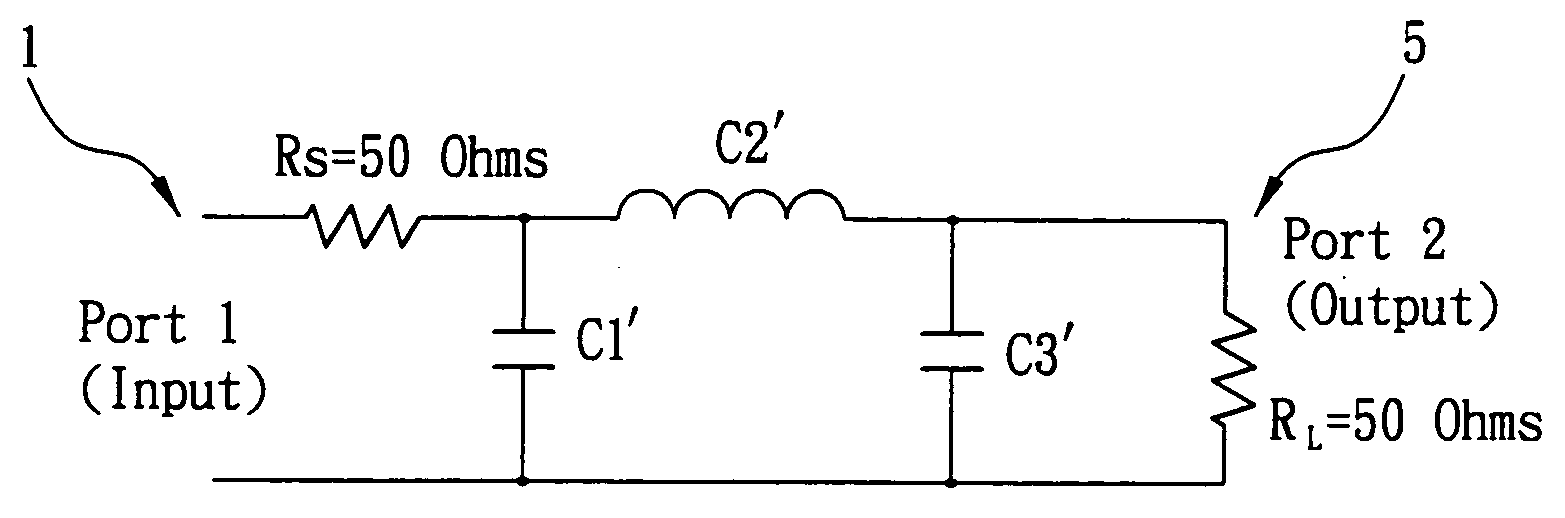
[0020] A first preferred embodiment of the invention directly distributes microwave circuits containing an input terminal, a resonant chamber of double frequencies, and an output terminal of a microwave filter on a circuit board of a wireless communication product to be produced by means of microstrip by utilizing the manufacturing technique of printed circuit board. The produced microwave filter is able to eliminate the harmonic spurious of double frequencies and the harmonic spurious of higher frequency caused by nonlinear distortion of a power amplifier of the wireless communication product. A π-section, low pass filter having an equal ripple of 0.5 dB is used as the prototype in designing the microwave filter of the invention. As shown in the equivalent circuit of FIG. 2, resistor value of resistor Rs in input terminal 1 or resistor RL in output terminal 5 is 50 Ohms. Also, g1=1.5963, g2=1.0967, g3=1.5963, and g4=1 by referring to David M. Pozar “Microwave Engineering” 2nd editi...


PUM


Abstract

The present invention is to provide a microwave filter distributed on a circuit board of a wireless communication product, which comprises an input terminal, a resonant chamber of double frequencies, and an output terminal of the microwave filter directly distributed on the circuit board of the wireless communication product as a plurality of microstrips by utilizing a manufacturing technique of printed circuit board for eliminating the harmonic spurious of double frequencies and higher frequency caused by nonlinear distortion of a power amplifier of the wireless communication product.

Description

FIELD OF THE INVENTION [0001] The present invention relates to wireless communication products and more particularly to an improved microwave filter distributed on the circuit board of a wireless communication product. BACKGROUND OF THE INVENTION [0002] Over the past several years there has been a simultaneous growth in the wireless communication product market, leading to an increasing use of WLAN (wireless local area network). One particularly important thing was the publication of IEEE 802.11 WLAN protocol in 1997. The WLAN protocol not only provides many novel features of WLAN communication but also provides a solution for communicating among various wireless communication products. This is a milestone for the development of WLAN. The WLAN protocol also ensures a solution of performing a single chip by means of core device and greatly reduces the cost of employing wireless technique. As a result, WLAN is readily adapted to employ in a variety of wireless communication products. ...

Claims


Application Information

Patent Timeline
Patent Type & Authority Applications(United States)
IPC IPC(8): H01P1/203H04B1/28H05K1/02H05K1/11H05K1/16
CPCH01P1/2039H05K1/0233H05K1/115H05K2201/1006H05K2201/09627H05K2201/0979H05K1/165
Inventor YANG, KUEI-CHI
Owner ALPHA NETWORKS INC
Why Eureka
Try Eureka