TSV structure applicable to adapter board and preparation method of TSV structure

An adapter plate and substrate technology, applied in semiconductor/solid-state device manufacturing, electrical components, electrical solid-state devices, etc., can solve the problems of increased cost, high etching cost, and small etching options

Active Publication Date: 2013-12-04
NAT CENT FOR ADVANCED PACKAGING
View PDF4 Cites 9 Cited by
  • Summary
  • Abstract
  • Description
  • Claims
  • Application Information

AI Technical Summary

Problems solved by technology

When TSV uses a single insulating layer, in the subsequent outcropping process, due to the requirements of etching depth and etching rate, the etching solution often needs to use hydrofluoric acid + nitric acid + acetic acid/deionized water (HNA) system, However, this solution system will also etch the silicon dioxide (TEOS) insulating layer, and the etching options for silicon and TEOS are relatively small. Once the TEOS insulating layer is etched, the diffusion barrier layer Ti or TiN will be exposed to the etching process. In the sol...

Method used


Image

  • TSV structure applicable to adapter board and preparation method of TSV structure
  • TSV structure applicable to adapter board and preparation method of TSV structure
  • TSV structure applicable to adapter board and preparation method of TSV structure

Examples


Embodiment 1

[0026] Embodiment 1: A method for preparing a TSV structure suitable for an adapter plate, comprising the following steps:

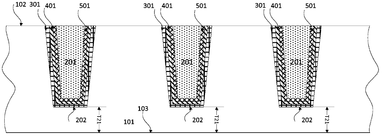
[0027] (1) if figure 1 As shown, a substrate 101 is provided, and the substrate 101 is a silicon wafer, silicon carbide (SiC) or gallium arsenide (GaAs), etc., and the substrate 101 has a corresponding substrate front 102 and a substrate back 103; TSV deep hole 201 is formed on 101, and the method of forming TSV deep hole 201 is deep reactive ion etching (DRID), reactive ion etching (RIE) or laser (laser); One end is the TSV head 202, and the thickness of the TSV head 202 from the back surface 103 of the substrate is T21; then a first insulating layer 301 is deposited on the front surface 102 of the substrate, and the first insulating layer 301 covers the front surface 102 of the substrate and the TSV deep hole 201 The side wall and the bottom wall of the first insulating layer 301 adopt thermal oxidation to grow silicon dioxide, and its thickness depen...

Embodiment 2

[0030] Embodiment 2: A method for preparing a TSV structure suitable for an adapter plate, comprising the following steps:

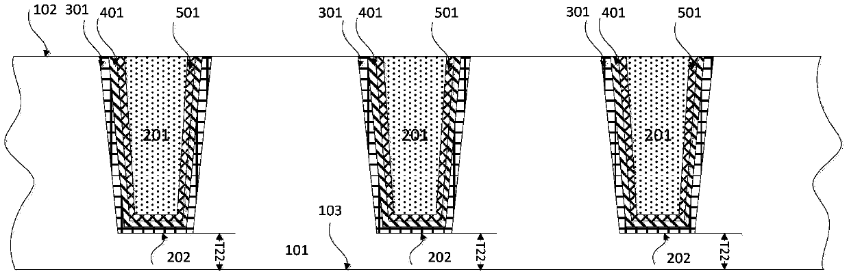
[0031] (1) if figure 1 As shown, a substrate 101 is provided, and the substrate 101 is a silicon wafer, silicon carbide (SiC) or gallium arsenide (GaAs), etc., and the substrate 101 has a corresponding substrate front 102 and a substrate back 103; TSV deep hole 201 is formed on 101, and the method of forming TSV deep hole 201 is deep reactive ion etching (DRID), reactive ion etching (RIE) or laser (laser); One end is the TSV head 202, and the thickness of the TSV head 202 from the back surface 103 of the substrate is T21; then a first insulating layer 301 is deposited on the front surface 102 of the substrate, and the first insulating layer 301 covers the front surface 102 of the substrate and the TSV deep hole 201 The side wall and the bottom wall of the first insulating layer 301 adopt thermal oxidation to grow silicon dioxide, and its thickness depen...

Embodiment 3

[0034] Embodiment 3: A method for preparing a TSV structure suitable for an adapter plate, comprising the following steps:

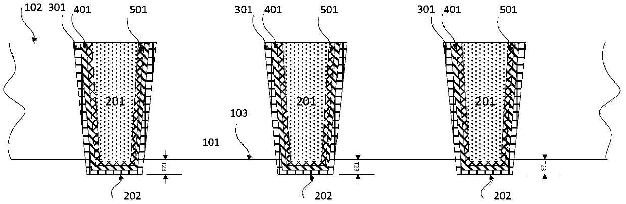
[0035] (1) if figure 1 As shown, a substrate 101 is provided, and the substrate 101 is a silicon wafer, silicon carbide (SiC) or gallium arsenide (GaAs), etc., and the substrate 101 has a corresponding substrate front 102 and a substrate back 103; TSV deep hole 201 is formed on 101, and the method of forming TSV deep hole 201 is deep reactive ion etching (DRID), reactive ion etching (RIE) or laser (laser); One end is the TSV head 202, and the thickness of the TSV head 202 from the back surface 103 of the substrate is T21; then a first insulating layer 301 is deposited on the front surface 102 of the substrate, and the first insulating layer 301 covers the front surface 102 of the substrate and the TSV deep hole 201 The side wall and the bottom wall of the first insulating layer 301 adopt thermal oxidation to grow silicon dioxide, and its thickness depen...


PUM


Abstract

The invention relates to a TSV structure applicable to an adapter board and a preparation method of the TSV structure. The TSV structure comprises a substrate and is characterized in that TSV deep holes are formed in the substrate, the side wall and the bottom wall of each TSV deep hole are provided with first insulating layers, second insulating layers are arranged on the surfaces of the first insulating layers, diffusion blocking layers are arranged on the surfaces of the second insulating layers, seed layers are arranged on the surfaces of the diffusion blocking layers, and the TSV deep holes are filled with conductive metal. The preparation method of the TSV structure applicable to the adapter board comprises the following steps that (1) the substrate is etched to form the TSV deep holes; (2) silicon dioxide is grown on the front surface of the substrate in a thermal oxidation mode so that the first insulating layers can be obtained, TEOS is deposited on the surfaces of the first insulating layers by adopting PECVD or SACVD or APCVD so that the second insulating layers can be obtained, then, the diffusion blocking layers are deposited on the surfaces of the second insulating layers, the seed layers are deposited on the surfaces of the diffusion blocking layers, and finally, the TSV deep holes are filled with the conductive metal. The TSV structure applicable to the adapter board is simple in process, low in cost and good in quality, and improves uniformity and insulativity of the insulating layers of silicon via holes.

Description

technical field [0001] The invention relates to a TSV structure suitable for an adapter board and a preparation method thereof, in particular to a microelectronic packaging technology / through-silicon via (TSV) structure of a semiconductor or solid device. Background technique [0002] TSV stands for Through Si via in the field of semiconductor microelectronics. In the process of 3D IC packaging and MEMS packaging, due to the use of multi-layer chip interconnection, it is necessary to punch holes through the entire chip to achieve electrical connection. [0003] The development of integrated circuits in terms of integration has always followed "Moore's Law", and as integrated circuit technology entered the era of 32nm technology, the complexity of the system and the investment cost of equipment have risen sharply, and the continuity of "Moore's Law" has been seriously affected. restrict. Meanwhile, conventional 2D miniaturization strategies have reached the limits of perfor...

Claims


Application Information

Patent Timeline
IPC IPC(8): H01L23/538H01L21/768
Inventor 王磊张文奇
Owner NAT CENT FOR ADVANCED PACKAGING
Why Eureka
Try Eureka