Very low power analog compensation circuit

A compensation circuit, integrated circuit technology, applied in the direction of power supply lines, logic circuits, electrical components, etc., can solve the problems of less general reference current, increased manufacturing cost, energy consumption of voltage conversion, etc.

Inactive Publication Date: 2009-07-15
SYNOPSYS INC
View PDF2 Cites 10 Cited by
  • Summary
  • Abstract
  • Description
  • Claims
  • Application Information

AI Technical Summary

Problems solved by technology

However, this approach has the disadvantages of dissipating a lot of energy through voltage conversion and generating the reference current in a less general way
Using high precision or trimmed external resistors also has the disadvantage of increasing manufacturing cost

Method used


Image

  • Very low power analog compensation circuit
  • Very low power analog compensation circuit
  • Very low power analog compensation circuit

Examples


Embodiment Construction

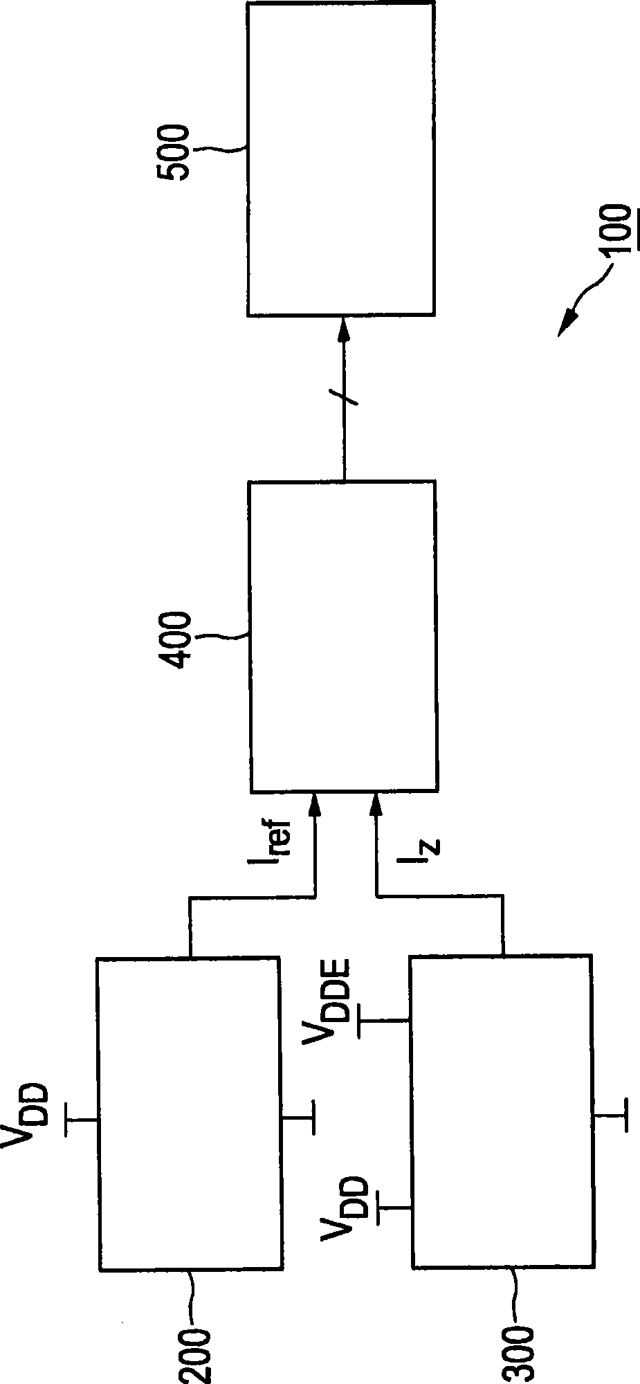
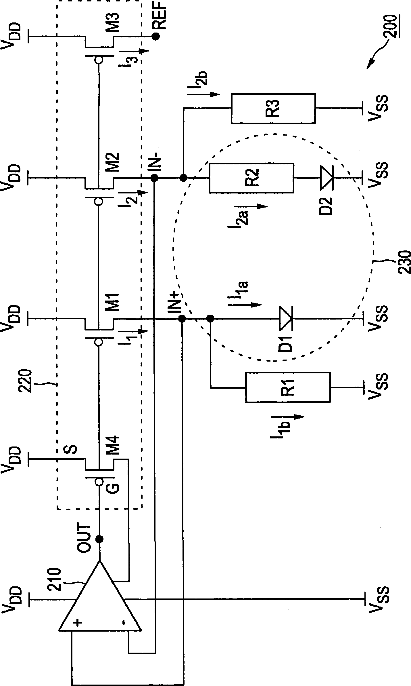
[0032] figure 2 is a block diagram of the compensation circuit 100 for the buffer circuit 500 according to the preferred embodiment of the present invention. The low power reference current source 200 is drawn from the reference low voltage source V DD (like a digital core voltage source, eg, which is present in every integrated circuit, with a constant value in the range of around 1.0V) directly generates the reference current I ref , the reference current I ref Defined as constant current over PVT variation. The sensing circuit 300 operates from a low voltage source (V DDE -V DD ) to generate the detection current I z , detection current I zis a variable current with PVT, the configuration of the sensing circuit 300 is based on the current transmitter 310, the low voltage source (V DDE -V DD ) with the reference high voltage source V DDE (such as high input / output (I / O) voltage sources in the range, for example, 1.8V to 2.5V) versus lower voltage sources (V DD ) c...


PUM


Abstract

The present invention relates to a compensation circuit for providing compen- sation over PVT variations within an integrated circuit. Using a low voltage reference current source, the compensation circuit generates directly, from an on-chip reference low voltage supply (VDD), a reference current (Iref) that is constant over PVT variations, whereas a detection current (Iz) that is variable over PVT variations is generated by a sensing circuit, which is based on a current conveyor, from a low voltage supply (VDDE-VDD) applied across a single diode-connected transistor (M10) corresponding to a voltage difference between two reference low voltage supplies. Both currents (Iref, Iz) are then compared inside a current mode analog-to-digital converter that outputs a plurality of digital bits. These digital bits can be subsequently used to compensate for PVT variations in an I / O buffer circuit.

Description

technical field [0001] The present invention relates to an analog compensation circuit, and more particularly, to a very low power analog compensation circuit for providing compensation for process, voltage and temperature (PVT) variations within an integrated circuit. Background technique [0002] Output buffer circuits (e.g., input / output (I / O) circuits) are widely used to facilitate the transfer of data and / or signals from one component to another on a given chip, or from one chip to another, where Route it using links or transmission lines such as buses, printed circuit board (PCB) traces, or any other conductive similar structures. [0003] Due to the increasing speed of integrated circuits (ICs), these links today are transmission lines that require their characteristic impedance (typically ranging from 50 ohms to 75 ohms) to be continuously matched to the impedance of the output buffer circuit or transmitter to avoid undesirable Reflection and shock excitation (ringi...

Claims


Application Information

Patent Timeline
Patent Type & Authority Applications(China)
IPC IPC(8): H03K19/003
CPCY10S323/907H03K19/00384H03K19/003
Inventor 安迪·尼古瓦米歇尔·泽克里
Owner SYNOPSYS INC
Why Eureka
Try Eureka