High voltage P type SOI MOS transistor

A technology of oxide semiconductor and silicon-on-insulator, which is applied in the direction of semiconductor devices, electrical components, circuits, etc., can solve the problems of reducing bonding strength, manufacturing process complexity, and unfavorable heat dissipation of devices, so as to reduce power consumption and breakdown voltage The effect of increasing and reducing the substrate current

Inactive Publication Date: 2010-09-01
SOUTHEAST UNIV
View PDF0 Cites 0 Cited by
  • Summary
  • Abstract
  • Description
  • Claims
  • Application Information

AI Technical Summary

Problems solved by technology

However, it makes most of the buried oxide layer have a large thickness, which is not conducive to the heat dissipation of the device, and also reduces the bonding strength. In addition, the etching of a large number of grooves also brings the complexity of the entire manufacturing process.

Method used


Image

  • High voltage P type SOI MOS transistor
  • High voltage P type SOI MOS transistor
  • High voltage P type SOI MOS transistor

Examples


Embodiment Construction

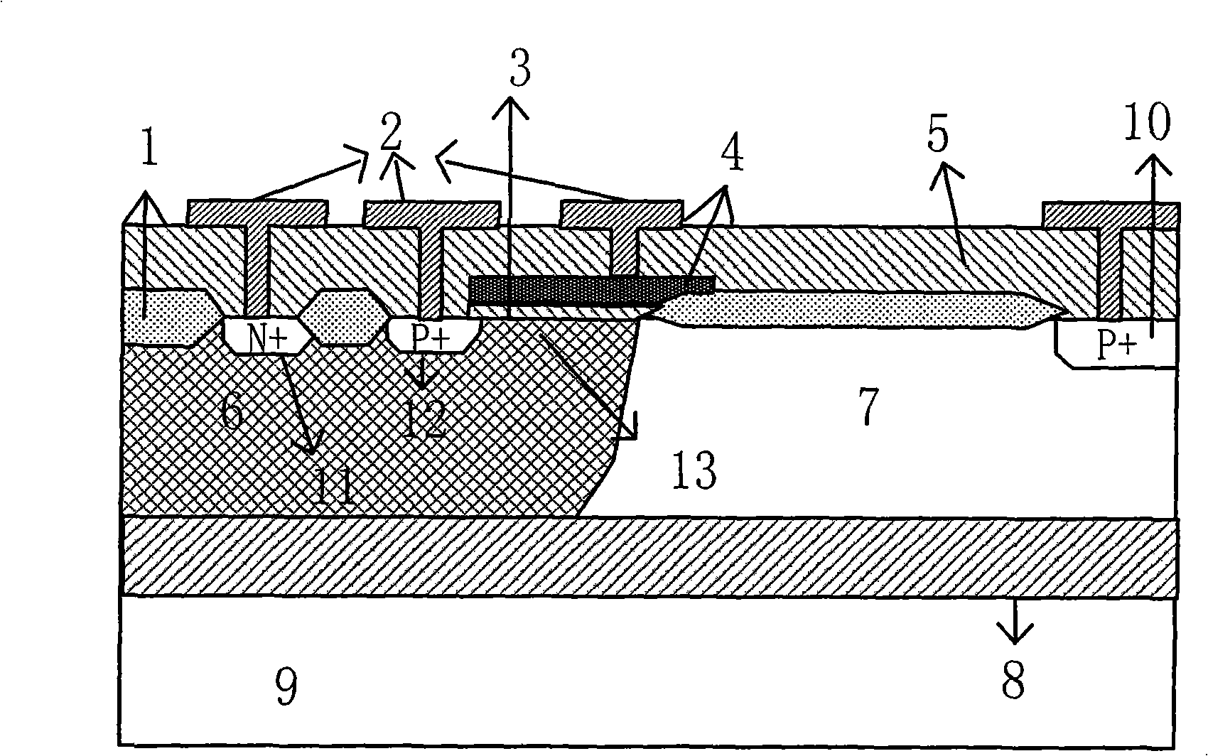
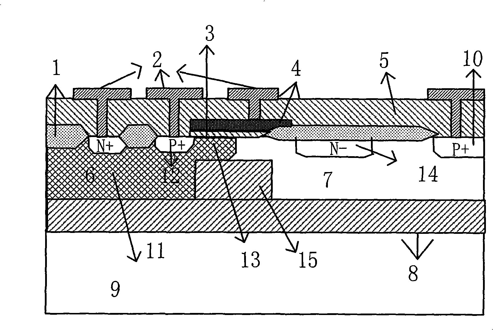
[0019] refer to figure 2 , a high-voltage P-type silicon-on-insulator metal oxide semiconductor tube, comprising: a semiconductor substrate 9, a buried oxide layer 8 is arranged on the semiconductor substrate 9, an N well 6 and a P-type well are arranged on the buried oxide layer 8 The doped semiconductor region 7 is provided with a P-type drain region 10 on the P-type doped semiconductor region 7, a P-type source region 12 and an N-type contact region 11 are provided on the N well 6, and a P-type drain region 10 is provided on the surface of the N well 6. The gate oxide layer 3 and the gate oxide layer 3 extend from the N well 6 to the P-type doped semiconductor region 7. On the surface of the N well 6, the P-type source region 12, the N-type contact region 11 and the area other than the gate oxide layer 3 and the P The area other than the P-type drain region 10 on the surface of the P-type doped semiconductor region 7 is provided with a field oxide layer 1, and a polysilico...


PUM


Abstract

A high voltage P type silicon-on-insulator metal oxide semiconductor pipe comprises a semiconductor substrate. An insulator buried oxide layer, a P type doped semiconductor area and an N well area are arranged on the semiconductor substrate, while a field oxide layer, a metal layer, a gate oxide, a polysilicon gate and an oxide layer are arranged on the surface of the device. The metal oxide semiconductor pipe is characterized in that a barrier oxide layer is arranged on a buried oxide layer and is positioned below the gate oxide; a channel area is formed between the barrier oxide layer and gate oxide; an N type inversion layer is arranged in the P type doped semiconductor area and is positioned on the lower surface of the field oxide layer between a P type drain area and a P type source area. With such a structure, electrons induced on an interface where the P type doped semiconductor area is connected with the buried oxide layer gather on the bottom of the P type doped semiconductorarea, greatly increasing the charge density at the interface, therefore, a thinner buried oxide layer can bear higher vertical breakdown voltage.

Description

Technical field: [0001] The present invention relates to the field of power semiconductor devices, and more specifically, relates to a structure of a silicon-on-insulator metal oxide semiconductor (SOI LDMOS) suitable for high-voltage applications. Background technique: [0002] Since the device made of silicon-on-insulator material can realize full dielectric isolation, its parasitic capacitance and leakage current are small, and the driving current is large, so it is very suitable for manufacturing power integrated circuits and devices. In order to make silicon-on-insulator devices work better, it is an important research topic to improve the breakdown voltage of silicon-on-insulator devices. As we all know, the withstand voltage of a silicon-on-insulator power device depends on the minimum of its lateral withstand voltage and vertical withstand voltage. The lateral withstand voltage of the device can be achieved by using bulk silicon junction termination technologies such...

Claims


Application Information

Patent Timeline
Patent Type & Authority Patents(China)
IPC IPC(8): H01L29/78
Inventor 孙伟锋贾侃吴虹钱钦松李海松陆生礼时龙兴
Owner SOUTHEAST UNIV
Why Eureka
Try Eureka