
Signal delay circuit

A signal delay and signal technology, applied in the direction of electrical components, pulse processing, single output arrangement, etc., can solve the problems of increased transmission delay, etc., and achieve the effect of reduced design complexity, high delay time resolution, and less redesign time

Inactive Publication Date: 2009-08-05
IND TECH RES INST
View PDF0 Cites 6 Cited by
  • Summary
  • Abstract
  • Description
  • Claims
  • Application Information

AI Technical Summary

Problems solved by technology

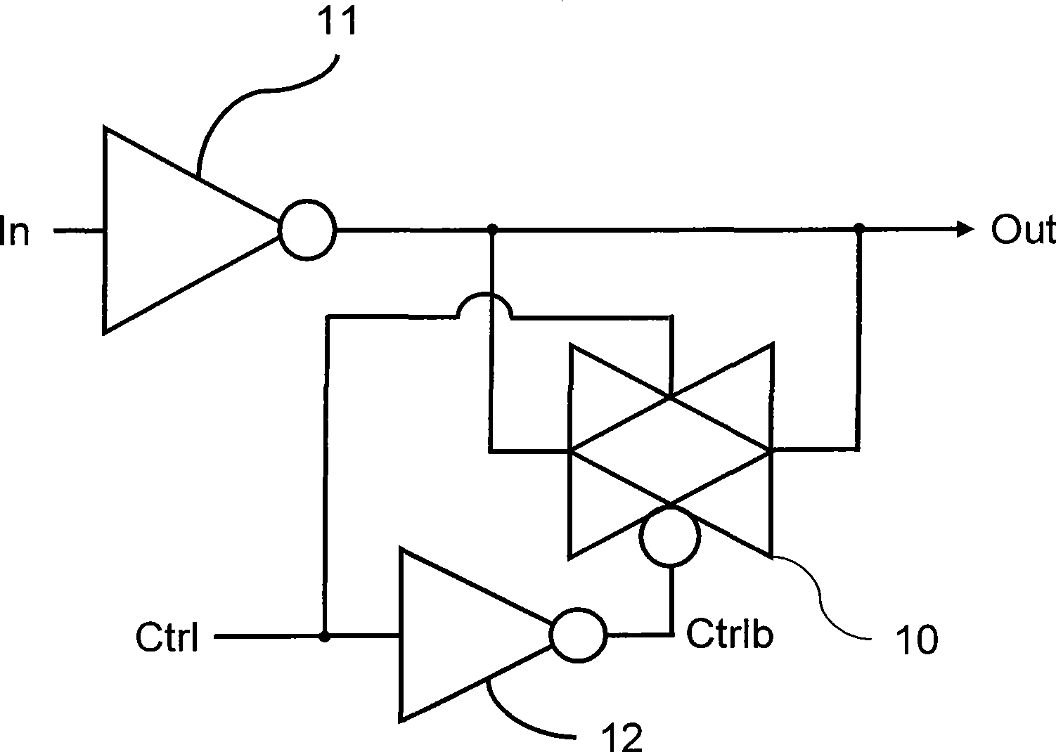
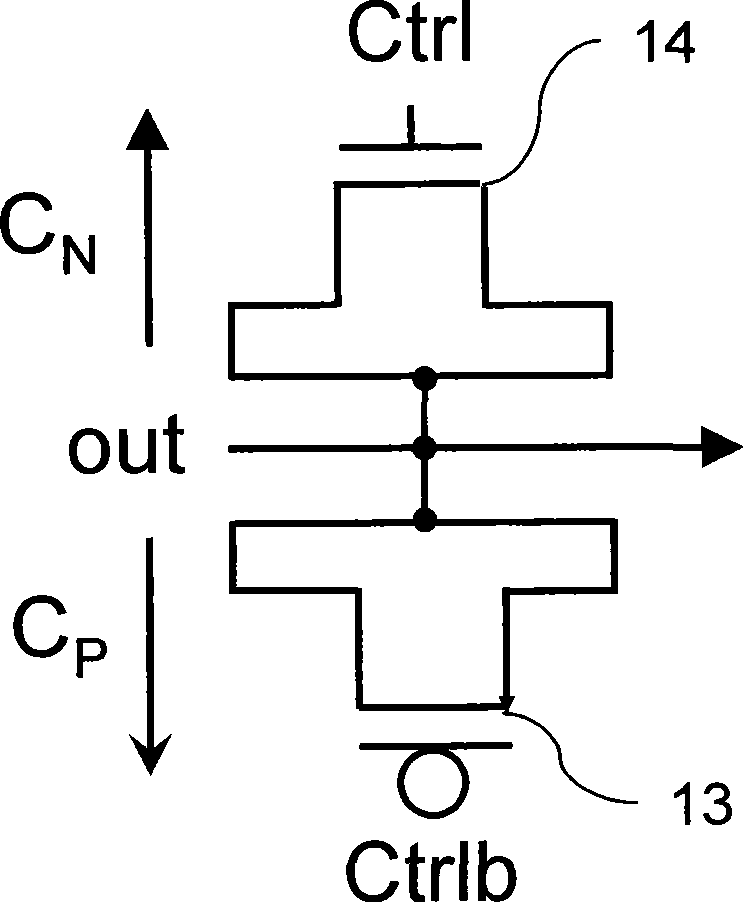
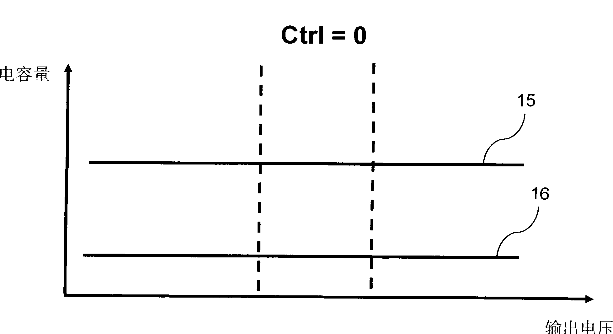
It can be seen from the figure that due to the change of the control signal, the transmission delay of this circuit will increase due to the increase of the parasitic capacitance value

Method used


Image

  • Signal delay circuit
  • Signal delay circuit
  • Signal delay circuit

Examples


Embodiment Construction

[0140] Please refer to Figure 7A and Figure 7B , is a schematic diagram of a signal delay circuit disclosed in an embodiment of the present invention. The signal delay circuit disclosed in the embodiment consists of a capacitive load element, in this embodiment a logic gate 100 with three input terminals. This logic gate 100 is composed of at least three switches 105 , 106 , 107 . In an embodiment, transistors can be used as the switches 105 , 106 , 107 . The resistors in the figure represent the equivalent parasitic resistances 101 , 102 , 103 , 104 of other active components or passive components in the logic gate. The voltages V1 and V2 can be power supply voltage or ground voltage.

[0141] exist Figure 7A In the illustrated embodiment, the switch 105 receives a first signal Sin, the switch 106 receives a second signal Inb, and the switch 107 receives a control signal Ctrl. The first signal Sin and the second signal Sinb are mutually inversion signals. In an embo...


PUM


Abstract

The invention discloses a signal delay circuit, comprising a capacitance load component. The component is provided with a first input end, a second input end and a third input end; wherein, the first input end receives a first signal; the second input receives a second signal which is an inversion signal of the first signal; and the third input end receives a control signal; wherein, the capacitance value of the capacitance load component is changed with the control signal.

Description

technical field [0001] The invention discloses a capacitive load component, in particular to a capacitive load component used in a signal delay circuit. Background technique [0002] Regarding the digital control delay circuit (digital control delay element), it can be divided into an analog delay circuit and a digital delay circuit in terms of structure and adjustment mechanism. [0003] The analog delay circuit is characterized by an analog control signal plus an analog delay circuit. A common analog delay circuit includes a digital-to-analog circuit and a delay circuit. The digital control signal converts the external digital control signal into an analog voltage through a digital to analog conversion circuit (Digital to Analog Converter, DAC). The delay circuit is composed of a differential pair circuit composed of N-type transistors or P-type transistors with different load resistors or load capacitors. By slightly adjusting the parameters in the delay component, such...

Claims


Application Information

Patent Timeline
IPC IPC(8): H03K5/13H03K5/14H03K5/133
Inventor 吕鸿文苏朝琴
Owner IND TECH RES INST
Learn More