Receiving chip circuit and communication system

A technology of receiving chips and circuits, applied in the field of communications, can solve the problems of dielectric loss, skin effect loss, and high price, and achieve the effect of increasing the rise rate, ensuring stable operation, and reducing the rise time.

Active Publication Date: 2013-03-13
BEIJING XINWANG RUIJIE NETWORK TECH CO LTD
View PDF0 Cites 0 Cited by
  • Summary
  • Abstract
  • Description
  • Claims
  • Application Information

AI Technical Summary

Problems solved by technology

In this case, it is usually necessary to choose a clock chip with better quality, but the price of this chip is higher, which increases the cost of the communication system
[0005] The second is that the rise time of the output signal of the clock chip can meet the requirements of the working chip of the communication system. However, due to the attenuation of the long-distance transmission line, the rise speed of the clock signal is degraded.
There are two losses in signal transmission on the transmission line: the first is the skin effect loss, that is, the energy lost because the current of the high-speed signal is only distributed on the edge of the transmission line
The second is dielectric loss, that is, when the signal is transmitted on the transmission line, some energy will enter the dielectric layer, causing the medium to heat and lose energy
This increases the cost of the communication system and the complexity of the product structure, and increases the design difficulty of the communication system product

Method used


Image

  • Receiving chip circuit and communication system
  • Receiving chip circuit and communication system
  • Receiving chip circuit and communication system

Examples


Embodiment Construction

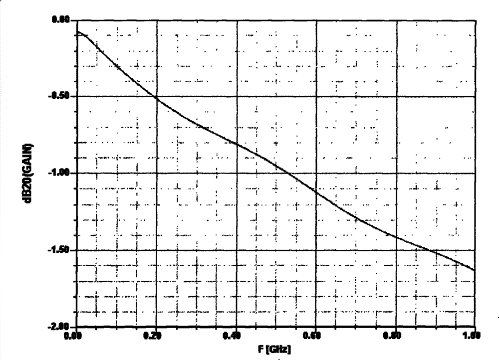
[0028] The ideal clock signal is composed of odd-order sine waves. For example: an ideal clock signal of 1MHz can be decomposed into a sinusoidal signal with infinite multiples such as 1 frequency, 3 frequency, 5 frequency, 7 frequency, 9 frequency, etc. Among them, 1 times the frequency is also called the fundamental frequency, 3 times frequency is also called the 3rd frequency, 5 times frequency is also called the 5th frequency, ... and so on. For an ideal clock signal, its energy is mainly concentrated on the 1st, 3rd and 5th harmonic signals. The higher the harmonic energy, the smaller the energy. When these harmonics are transmitted on the transmission line, the energy loss will not increase, and the higher the harmonics, the greater the energy loss.

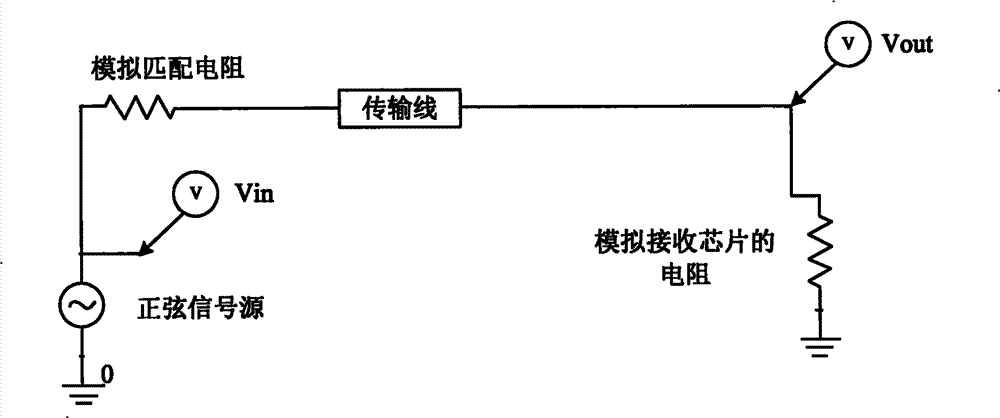
[0029] At present, when the impedance of the transmission line is 50 ohms, it is a good balance between manufacturability and performance. Such as figure 2 Shown. It is a schematic diagram of the simulation principle of th...


PUM


Abstract

The embodiment of the invention discloses a receiving chip circuit and a communication system; wherein, the receiving chip circuit comprises M receiving chips; in the M receiving chips, the input ends of N receiving chips are respectively provided with a regulating circuit which is used for gaining energy of clock signals input into the input end of the N receiving chips in a selected frequency band to a preset value; wherein, N is an integer which is more than zero and M is larger than N. The communication system comprises a PCB, which is provided with a clock chip and the receiving chip circuit; and the clock chip provides clock signals for the M receiving chips in the receiving chip circuit by transmission lines. The embodiment of the invention can effectively improve rising rate of the clock signals, reduce the rising time of the clock signals, meet the input requirements of working chips and guarantee the stable working of the working chips.

Description

Technical field [0001] The invention relates to communication technology, in particular to a receiving chip circuit and a communication system. Background technique [0002] In a communication system, for a large working chip, it is usually necessary to use at least one communication system clock provided by the outside, that is, a working clock, to perform work. With the advancement of communication technology and the gradual increase in communication requirements, the performance requirements of working chips for working clocks are getting higher and higher. Among the performance parameters of the working clock, a very important parameter is the rise time of the clock signal. Among them, the rise time of the signal refers to the time required for the signal to transition from low level to high level. At present, the industry generally uses the conversion time between 20% to 80% or 10% to 90% of the difference between the high level and the low level to define the signal rise ...

Claims


Application Information

Patent Timeline
Patent Type & Authority Patents(China)
IPC IPC(8): H04B1/16
Inventor 何冲
Owner BEIJING XINWANG RUIJIE NETWORK TECH CO LTD
Why Eureka
Try Eureka