Charge pump and CMOS image sensor

A technology of image sensor and charge pump, applied in image communication, TV, color TV, etc., can solve the problems of low efficiency and large area of ​​charge pump, and achieve the effect of improving efficiency

Inactive Publication Date: 2009-08-19
BRIGATES MICROELECTRONICS KUNSHAN
View PDF0 Cites 18 Cited by
  • Summary
  • Abstract
  • Description
  • Claims
  • Application Information

AI Technical Summary

Problems solved by technology

[0009] The problem to be solved by the present invention is that the efficien

Method used


Image

  • Charge pump and CMOS image sensor
  • Charge pump and CMOS image sensor
  • Charge pump and CMOS image sensor

Examples


Embodiment Construction

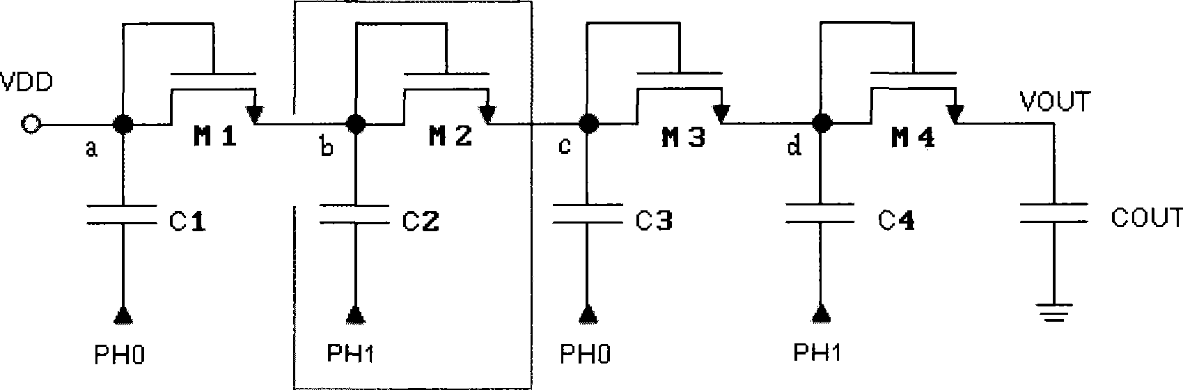
[0022] Through the analysis of the working process of the current Dickson charge pump, it can be obtained that in a certain clock (PH0 or PH1) in the Dickson charge pump, only one phase has charge pumped to the external capacitor COUT, so the efficiency is low. Moreover, the Dickson charge pump can only increase the voltage step by step through multiple boost stages in order to achieve the voltage required for driving the pixels of the CMOS image sensor, which will inevitably increase the capacitor area. Therefore, the boost stage structure of the current Dickson charge pump limits its boost boost efficiency and area reduction.

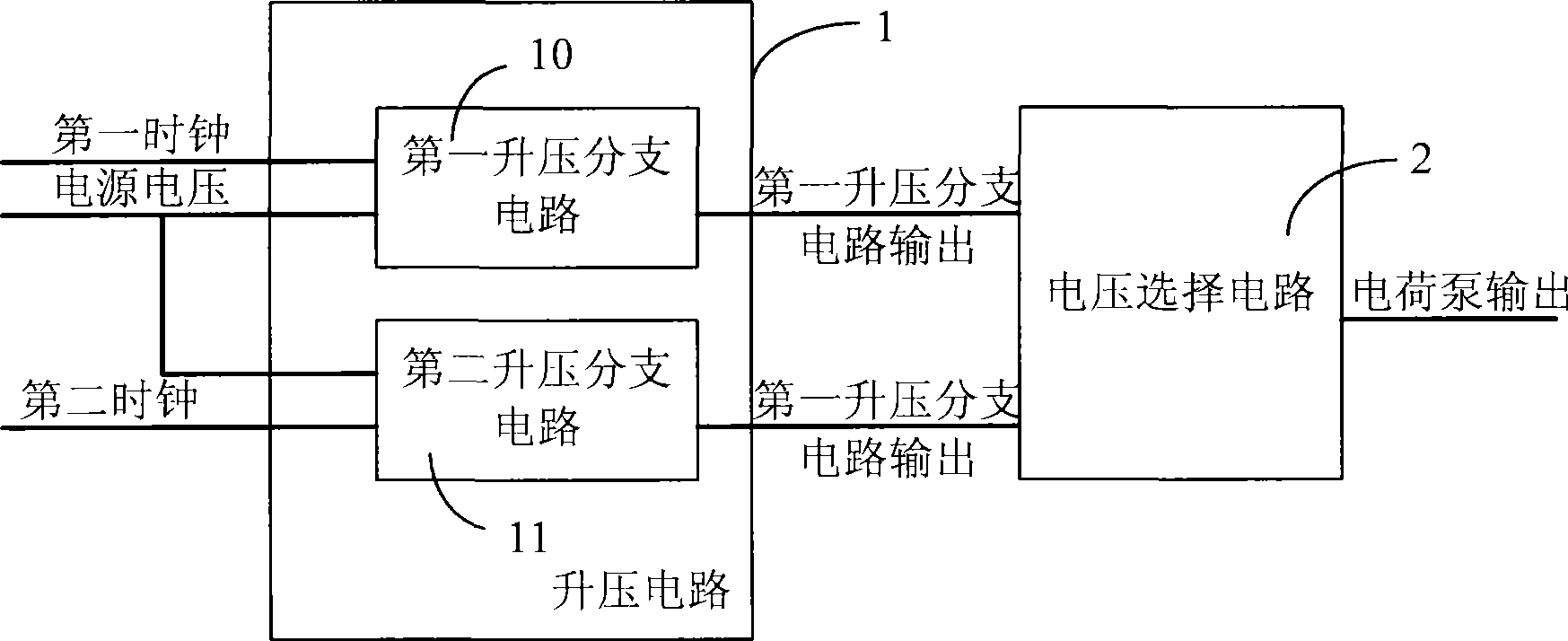
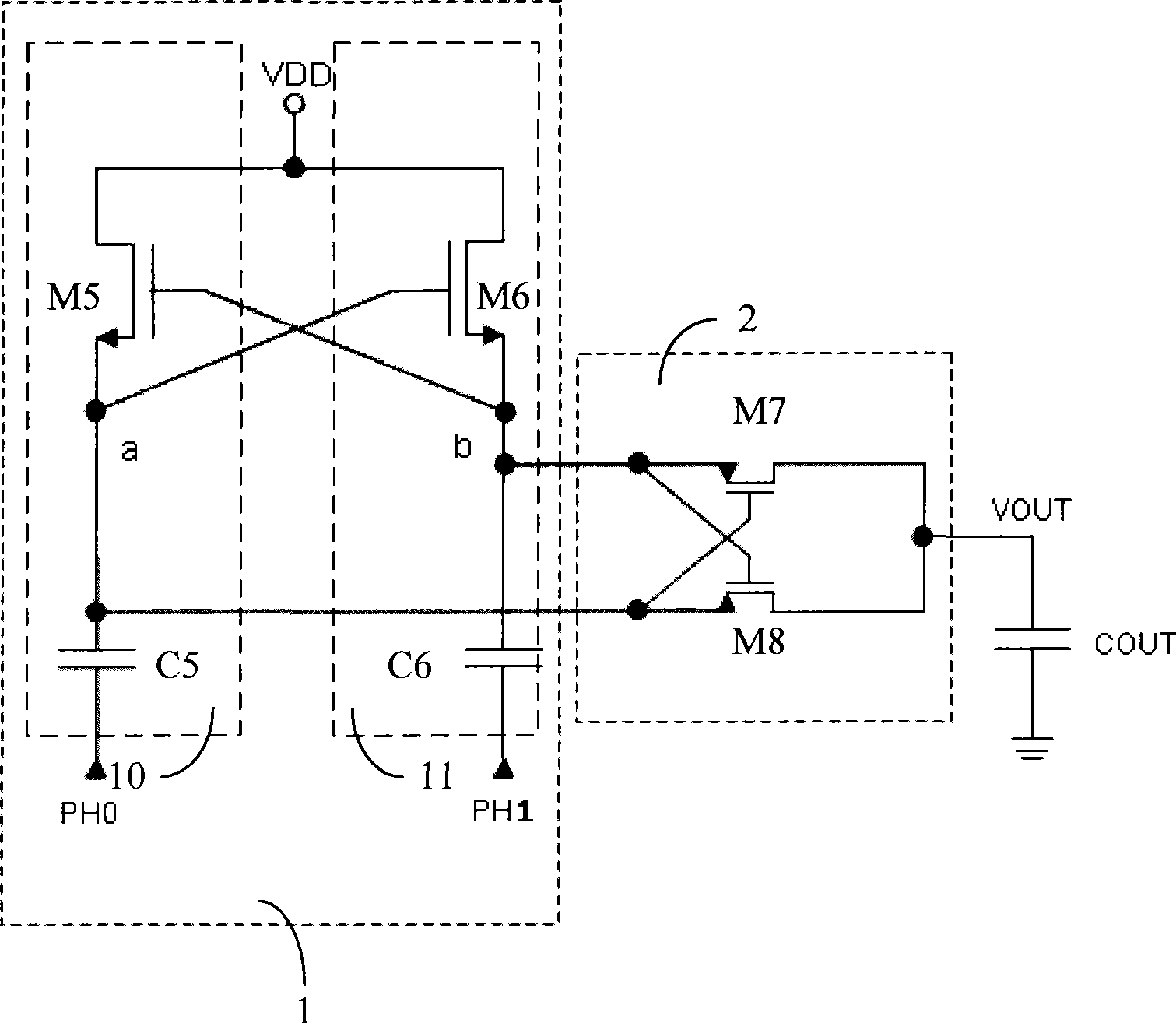
[0023] Therefore, in view of the above problems, a feasible method is to enable the charge pump to boost the voltage in both phases of the clock (high-level phase and low-level phase), so as to improve the boosting efficiency accordingly, and can correspondingly increase the area. reduce. Based on this, an embodiment of the charge pump of the present...


PUM


Abstract

The invention discloses a charge pump and a CMOS image sensor; wherein the charge pump comprises: a boost circuit consisting of a first boost branch circuit and a second boost branch circuit which are connected with the power voltage; the first boost branch circuit and the second boost branch circuit are respectively controlled by a first clock and a second clock, which are a pair of non-overlap clocks with adverse phases, wherein, when the first clock is in the first phase, the first boost branch circuit realizes the boost of the power voltage; when the second clock is in the first phase, the second boost branch circuit realizes the boost of the power voltage; the voltage chooses the circuit, coupling to the first boost branch circuit and the second boost branch circuit, and forms the output of the charge pump through the output of the boost branch circuit of boost power voltage. The charge bump has high conversion rate, smaller waves and smaller area occupied.

Description

technical field [0001] The present invention relates to a complementary metal oxide semiconductor (CMOS) image sensor, in particular to a charge pump for driving pixels of the CMOS image sensor and a corresponding CMOS image sensor with the charge pump. Background technique [0002] Image sensors are semiconductor devices used to convert optical images into electrical signals, including Charge Coupled Device (CCD, Charge Coupled Device) image sensors and Complementary Metal Oxide Semiconductor (CMOS) image sensors. [0003] Among them, the CMOS image sensor adopts CMOS technology using a control circuit and a signal processing circuit as peripheral circuits, and also adopts a switching technology that allows sequential detection of output using MOS transistors arranged corresponding to the number of pixels arranged to thereby detect an image. In addition, CMOS image sensors utilize CMOS manufacturing technology. [0004] CMOS image sensors generally require the use of charg...

Claims


Application Information

Patent Timeline
IPC IPC(8): H02M3/07H04N5/335
Inventor 罗文哲陈巨
Owner BRIGATES MICROELECTRONICS KUNSHAN
Why Eureka
Try Eureka