Electrochemically active organic thin film, method for producing the same, and device using the same

An organic thin film, electrochemical technology, applied in the field of electrochemically active organic thin films, can solve the problems of difficulty in building electronic circuits and low response speed

Inactive Publication Date: 2009-08-19
TOYOTA JIDOSHA KK
View PDF0 Cites 7 Cited by
  • Summary
  • Abstract
  • Description
  • Claims
  • Application Information

AI Technical Summary

Problems solved by technology

[0004] However, 30 years after it was first proposed, it is still difficult to construct electronic circuits composed of organic molecules
Despite the steady progress of this technology, the chances of practical application of molecular semiconductors that can replace metal wires with a response speed comparable to that of highly conductive molecular wires, silicon or compound semiconductors, etc., are still very low in the near future.

Method used


Image

  • Electrochemically active organic thin film, method for producing the same, and device using the same
  • Electrochemically active organic thin film, method for producing the same, and device using the same
  • Electrochemically active organic thin film, method for producing the same, and device using the same

Examples


Embodiment Construction

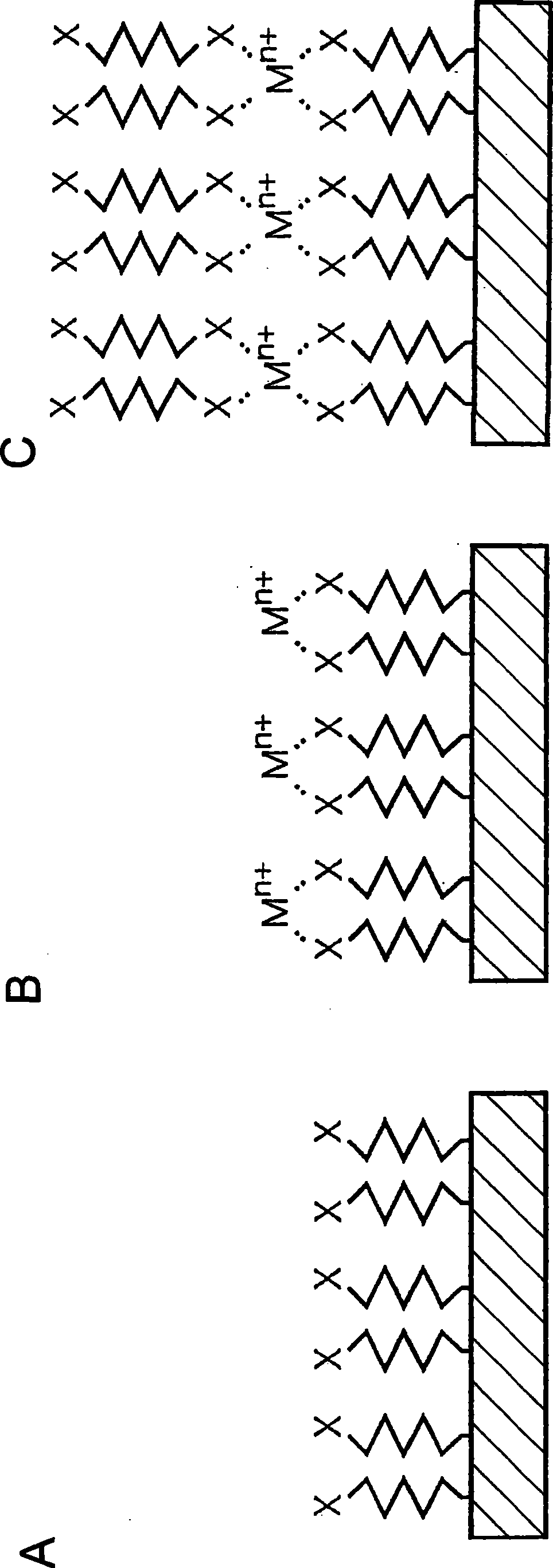
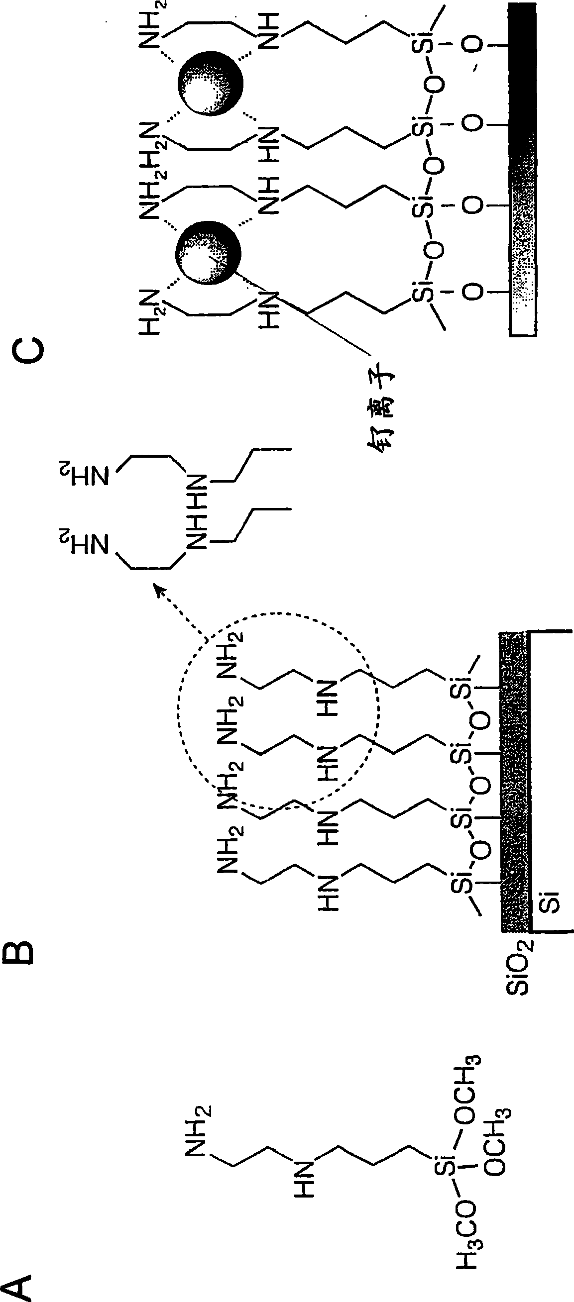
[0043] When a hydrogen-terminated silicon surface undergoes thermal / photoexcitation, the hydrogen atoms on the surface are removed and silicon radicals are generated. Through the reaction between silicon radicals and organic molecules, silicon radicals combine with organic molecules to form a monolayer. In the case of the reaction between silicon radicals and unsaturated hydrocarbons, organic molecules such as alcohol molecules or aldehyde molecules are immobilized on the silicon substrate through Si—C bonds, and a monolayer is formed. The reaction temperature is between 100°C and 200°C; however, it is very unlikely that Si-H bonds will be split and hydrogen atoms will be removed at such low temperatures. Therefore, the removal of the hydrogen atom is considered to proceed at a site where the hydrogen atom is easily removed for some reason, and the reaction is considered to proceed due to a chain reaction.

[0044] The method of immobilizing metal coordination compound molecu...


PUM

PropertyMeasurementUnit
thicknessaaaaaaaaaa
thicknessaaaaaaaaaa

Abstract

This invention provides an electrochemically active organic thin film capable of repeating reversible oxidation / reduction a number of times. Further, the invention provides a novel approach to so-called ''molecular nanoelectronics'' utilizing organic molecules as operating units, with the use of such organic thin film. Such electrochemically active organic thin film comprises a substrate, an organic molecular film comprising organic molecules having terminal amino groups chemically fixed on the surface of the substrate, and metal atoms or metal ions coordinately bound to the amino groups.

Description

technical field [0001] The present invention relates to electrochemically active organic thin films capable of repeating reversible oxidation / reduction multiple times, methods for their manufacture, and several devices using the same. Background technique [0002] The miniaturization of semiconductor integrated circuits (ICs) is continuing to progress. In 2005, mass production of super integrated circuits with a minimum line width of 65 nm became possible. The design rule of minimum line width of 22nm is the goal to be achieved in the next 10 years. Furthermore, in the near future, processing precision at the atomic and molecular level, such as process line widths of 10 nm or less, will be required. However, whether electronic devices for this single-nanotechnology era can be constructed using existing electronic materials, semiconductors, metals or dielectrics is a major concern. Therefore, a breakthrough in the field of materials engineering is expected. [0003] As a ...

Claims


Application Information

Patent Timeline
Patent Type & Authority Applications(China)
IPC IPC(8): G01N27/414G01N27/30
CPCH01L51/0545G01N27/414G01N27/307Y10T156/10Y10T428/31663H10K10/466
Inventor 别所毅杉村博之邑瀬邦明
Owner TOYOTA JIDOSHA KK
Why Eureka
Try Eureka