Pixel structure of liquid crystal display

A liquid crystal display, technology of pixel structure

Active Publication Date: 2009-09-09
HANNSTAR DISPLAY CORPORATION
View PDF0 Cites 8 Cited by
  • Summary
  • Abstract
  • Description
  • Claims
  • Application Information

AI Technical Summary

Problems solved by technology

[0006] Although the pixel structure 9 shown in FIG. 1 and FIG. 2 reduces the stray capacitance Cpd between the pixel electrode 96 and the data line 93 by setting the organic insulating layer 97, the second electrode between th

Method used


Image

  • Pixel structure of liquid crystal display
  • Pixel structure of liquid crystal display
  • Pixel structure of liquid crystal display

Examples


Embodiment approach

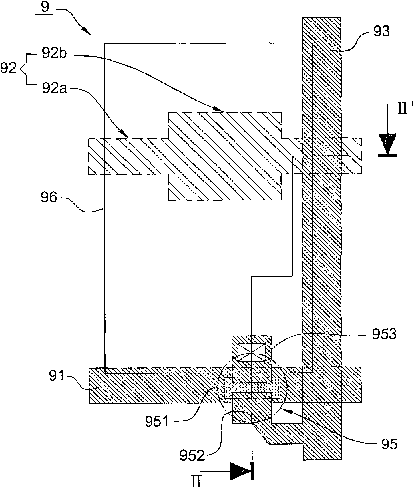
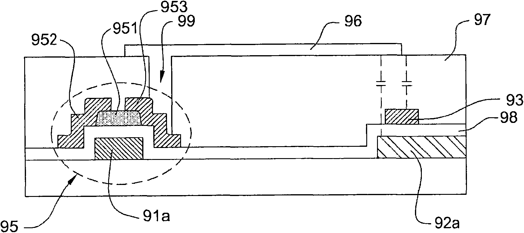
[0045] Please refer to Figure 9a, which shows the first implementation of the third embodiment of the present invention, the pixel structure 3 includes a substrate 10, such as a glass substrate; the transparent electrode 35 is directly formed on the substrate 10; the second part 12b of the wire 12 is formed on On the substrate 10, it partially overlaps and is electrically connected to the transparent electrode 35; a gate insulating layer 16 is deposited on the substrate 10 and covers the transparent substrate 35 and the second portion 12b of the lead 12; the first data line 13a and the second data line 13b are formed on the gate insulating layer 16, and the second data line 13b partially overlaps with the second portion 12b of the conductive line 12, wherein the first data line 13a and the second data line 13b is formed by the same photolithography process (the second metal layer); the inorganic passivation layer 17 is formed on the gate insulating layer 16 and covers the fir...


PUM


Abstract

The invention relates to a pixel structure of a liquid crystal display, which comprises a substrate, a shading part, a first data wire, a second data wire and a pixel electrode. The shading part is arranged on the substrate; the first data wire and the second data wire are arranged along the shading part; and the second data wire is partially overlapped with the shading part; and the pixel electrode is partially overlapped with the first data wire and the shading part, and not overlapped with the second data wire.

Description

technical field [0001] The invention relates to a pixel structure of a liquid crystal display, in particular to a pixel structure of a liquid crystal display with high aperture ratio and low data line coupling ratio. Background technique [0002] With the advancement of electronic technology, especially the prevalence of portable electronic products in daily life, the demand for display devices that are thin, light, small, and low in power consumption is increasing day by day. Liquid Crystal Display (LCD) devices are suitable for such electronic products due to their advantages of low power consumption, thin thickness, and light weight, and have even gradually replaced traditional cathode ray tube display devices. [0003] Since the aperture ratio of a pixel is an important factor affecting the characteristics of a liquid crystal display, various pixel structures have been proposed in the industry to increase the aperture ratio of a pixel. refer to Figure 11 And FIG. 2, FI...

Claims


Application Information

Patent Timeline
IPC IPC(8): G02F1/1362H01L27/12H01L21/60G02F1/1343
CPCH01L2924/0002
Inventor 张祖强施博盛陈柏仰吴昭慧
Owner HANNSTAR DISPLAY CORPORATION
Why Eureka
Try Eureka