Method for applying continuously adjustable uniaxial stress to semiconductor samples at low temperature

A semiconductor and sample technology, which is applied in the field of semiconductor wafer measurement, can solve the problems of unrecoverable samples and small degrees of freedom, and achieve the effects of good thermal conductivity, small size, and not easy to damage

Inactive Publication Date: 2010-12-08
INST OF SEMICONDUCTORS - CHINESE ACAD OF SCI
View PDF4 Cites 2 Cited by
  • Summary
  • Abstract
  • Description
  • Claims
  • Application Information

AI Technical Summary

Problems solved by technology

Although this method has very small requirements for the volume of the mechanical device, its limitations are obvious: the magnitude of the stress is dependent on the magnitude of the temperature, as well as the thermal expansion coefficient of the material itself, and the controllable degrees of freedom are very large. Small
Moreover, the sample cannot be recovered after the measurement is completed.

Method used


Image

  • Method for applying continuously adjustable uniaxial stress to semiconductor samples at low temperature
  • Method for applying continuously adjustable uniaxial stress to semiconductor samples at low temperature
  • Method for applying continuously adjustable uniaxial stress to semiconductor samples at low temperature

Examples


specific Embodiment

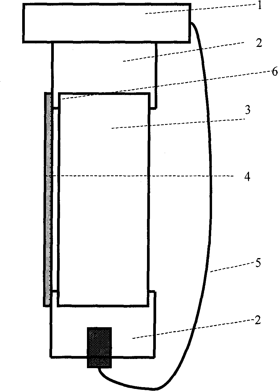
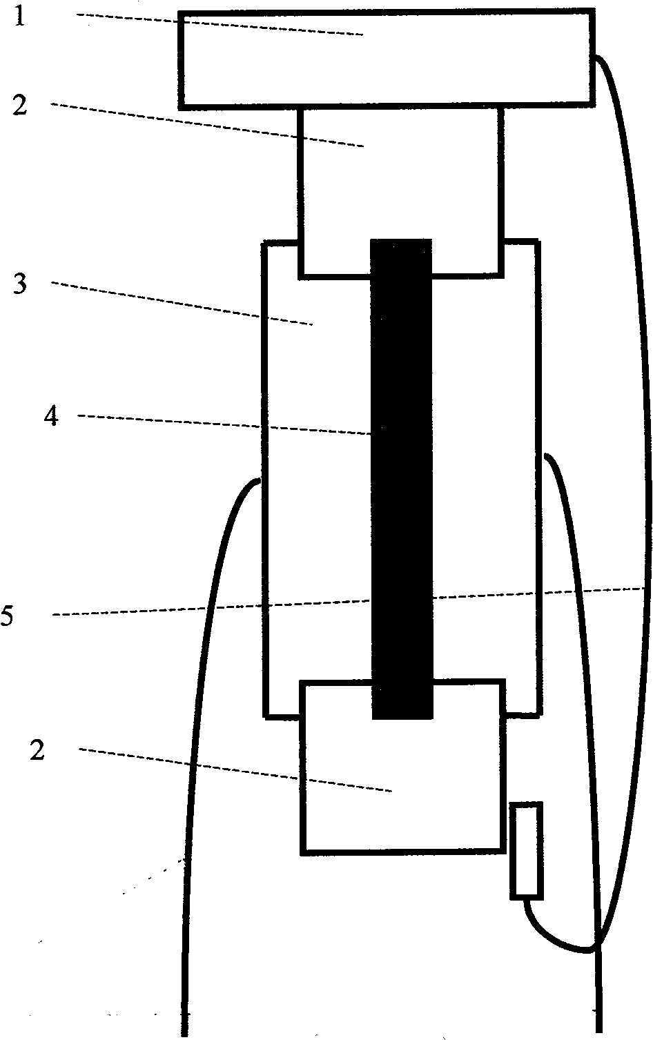
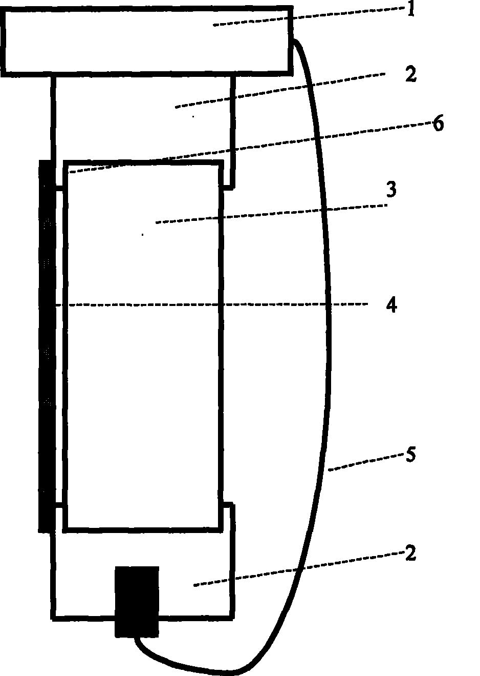
[0036] 1) Use the U-shaped red copper cap 2 with an overall size of 11×5×6.5mm, the depth of the groove is 2mm, the thickness of the outer walls on both sides of the groove is 0.5mm, and the size of the piezoelectric ceramic 3 is 5×5×9mm.

[0037] 2) Sample 4 is a GaAs / AlGaAs superlattice with a length of 7 mm, a thickness of 0.5 mm, 30 periods, and a GaAs / AlGaAs superlattice grown along the [001] direction. The substrate is GaAs, and the sample is cut along the [110] direction. Use the commercially available "Anteco" superglue to bond the two ends to the two copper caps 2, and then use a hair dryer to blow hot air on the bonding place for 15 minutes.

[0038] 3) Fix a red copper cap 2 on the heat transfer metal probe 1 of the small Dewar flask with screws, and use low-temperature vacuum grease at the joint to enhance contact and heat conduction.

[0039] 4) The other copper cap 2 is connected to the heat transfer probe 1 of the cryogenic device through the copper heat conduct...


PUM


Abstract

The invention provides a method for applying continuously adjustable uniaxial stress to semiconductor samples at a low temperature. The method comprises the following steps: choosing a piezoelectric ceramic actuator which can regulate applied stress by changing the bias voltage of piezoelectric ceramics; fixing two U-shaped red-copper blocks used at two ends of the piezoelectric ceramic actuator to fix samples and conduct heat; connecting a red-copper heat-conducting wire with one red-copper block to conduct heat uniformly and rapidly; using super glue to bond two ends of a semiconductor sample to the two U-shaped copper blocks; and changing the bias voltage of the piezoelectric ceramics on the piezoelectric ceramic actuator so as to apply continuously adjustable uniaxial stress to the semiconductor sample. The method has the advantages that the magnitude of uniaxial stress is continuously adjustable in double directions and can be measured; the sample is rapid and accurate in temperature reduction; and a device is small in occupied volume and easy to operate and can be perfectly combined with a low-temperature device.

Description

technical field [0001] The invention relates to the technical field of semiconductor wafer measurement. In particular, devices and methods for applying continuously adjustable uniaxial stress to semiconductor samples at low temperatures. Background technique [0002] The internal stress of semiconductors has a significant impact on the properties of the corresponding devices and structures. A large number of growth and processing processes are focused on how to eliminate or control the stress inside the substrate. Stress can have dramatic effects on the optical, electrical, magnetic, and a host of other properties of semiconductor materials. In the field of semiconductor detection technology, only when quantitative and measurable uniaxial stress can be applied to the sample can the relevant properties of semiconductor materials be accurately determined. In recent years, with the rise of superconductivity and a series of high-tech technologies, the precise application and ...

Claims


Application Information

Patent Timeline
Patent Type & Authority Patents(China)
IPC IPC(8): G01N19/00G01N3/00
Inventor 周振宇陈涌海
Owner INST OF SEMICONDUCTORS - CHINESE ACAD OF SCI
Why Eureka
Try Eureka