Unlock instant, AI-driven research and patent intelligence for your innovation.

Semiconductor encapsulation structure with pins on chip

A semiconductor and chip technology, applied in the direction of semiconductor devices, semiconductor/solid-state device parts, electric solid-state devices, etc., to achieve the effect of not easy to tilt and tilt, improve the anti-stress effect, and strengthen the locking ability.

Inactive Publication Date: 2010-10-20
POWERTECH TECHNOLOGY INC
View PDF6 Cites 0 Cited by
  • Summary
  • Abstract
  • Description
  • Claims
  • Application Information

AI Technical Summary

Problems solved by technology

However, such as Figure 2 and Figure 3, among these pins 110, the pins located on the outermost two sides The contact fingers 111A of the pin 110 will be subjected to relatively large stress, which is a stress concentration area, causing the outermost two contact fingers 111A to be easily delaminated with the chip 140 (eg Figure 3), so the layered contact finger 111A will touch the adjacent contact finger 111 during molding and thus cause electrical short circuit

Method used


Image

  • Semiconductor encapsulation structure with pins on chip
  • Semiconductor encapsulation structure with pins on chip
  • Semiconductor encapsulation structure with pins on chip

Examples


no. 1 Embodiment

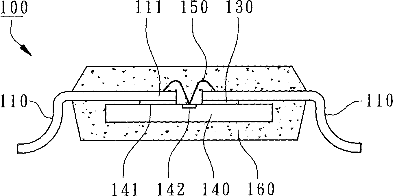
[0054]According to a first embodiment of the present invention, a lead-on-chip (LOC, Lead-On-Chip) semiconductor package structure is disclosed. Wherein, the "pins on the chip" referred to here means that the pins of the lead frame are attached to the active surface of the chip, so as to achieve the effect of carrying the chip during the packaging process. Figure 4 A schematic cross-sectional view along the pin centerline is constructed for the semiconductor package. Figure 5 is a schematic plan view of a lead frame suitable for the semiconductor package configuration. Figure 6 It is a schematic plan view of the leadframe after die bonding and wire bonding. Figure 7 for Figure 6 A zoomed-in view of a feature in a leadframe prior to wire bonding. Figure 8 A schematic partial cross-sectional view cut along the lead fingers is constructed for the semiconductor package. in, Figure 5 can be with figure 2 Compared with the known lead frames for feature differences, F...


PUM


Abstract

The invention discloses a semiconductor encapsulation structure with pins on a chip. The semiconductor encapsulation structure mainly comprises two or more pins of a lead frame, at least one connecting strip, an adhesive layer, the chip, two or more welding lines and an adhesive body for sealing the components. The connecting strip is provided with virtual joint fingers which are arranged at the lateral edges of two or more joint fingers of the pins and are in linear arrangement with the joint fingers. The adhesive layer is adhered to the lower surfaces of the joint fingers and the virtual joint fingers. The chip has an active surface, and the joint fingers and the virtual joint fingers are adhered to the active surface, so that the virtual joint fingers are close to a first edge of the active surface. The joint fingers are electrically connected with a welding pad of the chip. The invention also discloses a lead frame applicable to the semiconductor encapsulation structure with the pins on the chip. The virtual joint fingers are used to bear stress concentration action, so the joint fingers on the active surface avoid layering due to the stress.

Description

technical field [0001] The present invention relates to a semiconductor device, in particular to a lead-on-chip (LOC, Lead-On-Chip) semiconductor packaging structure. Background technique [0002] A semiconductor package (also called a semiconductor package) uses an encapsulant to seal the semiconductor chip to increase dust and moisture resistance. And the electrical signal of the chip can be led out by using the lead frame pins for external connection to external electrical components. The so-called "pins on the chip" means that the pins extend to the active surface of the chip and paste and fix the chip without using a chip holder. However, the die bonding and molding process of the entire semiconductor packaging process needs to undergo temperature cycle changes. Since the thermal expansion coefficient of the metal pin as the chip carrier is still different from that of the semiconductor chip, thermal stress will be generated, resulting in pins Where stress may concen...

Claims


Application Information

Patent Timeline
Patent Type & Authority Patents(China)
IPC IPC(8): H01L23/488H01L23/495H01L23/31
CPCH01L2224/4826H01L2224/48091H01L2224/32245H01L2224/73215
Inventor 范文正徐玉梅
Owner POWERTECH TECHNOLOGY INC