Blue-light top luminous organic diode structure and fabricating method thereof

A technology of light-emitting diodes and blue light-emitting layers, which is applied in the manufacture of semiconductor/solid-state devices, electrical components, and electric solid-state devices. The effect of simplifying the preparation process and enhancing the emission intensity

Inactive Publication Date: 2009-09-23
NANJING UNIV OF POSTS & TELECOMM
View PDF0 Cites 25 Cited by
  • Summary
  • Abstract
  • Description
  • Claims
  • Application Information

AI Technical Summary

Problems solved by technology

The former has higher requirements on the film-forming process of ITO and IZO, and it is easy to damage the organic layer at the bottom during the preparation of ITO and IZO films, resulting in short circuit of the device or large leakage current; Makes more and more research on top-emission OLEDs based on translucent metals
However, the problem with this type of OLED is that the highly reflective electrode at the bottom and the semi-transparent electrode at the top form a resonant cavity, and the change in the thickness of the resonant cavity has certain selectivity for the light color.
This method requires multi-step plate alignment procedures when making three primary color array pixels, which makes the OLED display manufacturing process complicated.

Method used


Image

  • Blue-light top luminous organic diode structure and fabricating method thereof
  • Blue-light top luminous organic diode structure and fabricating method thereof
  • Blue-light top luminous organic diode structure and fabricating method thereof

Examples


Embodiment Construction

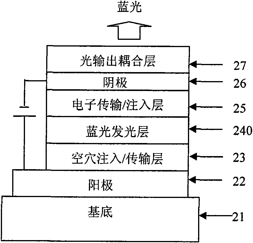
[0051] refer to image 3 , the structure of the blue top-emitting OLED device of the present invention includes a substrate 21, a reflective electrode (anode) 22, a hole injection / transport layer 23, a blue light emitting layer 240, an electron transport / injection layer 25, and a semitransparent metal electrode (cathode) 26 and light outcoupling layer 27. Among them, in this embodiment, the substrate, reflective electrode, hole injection layer, hole transport layer, blue light emitting layer, electron transport layer, electron injection layer, translucent metal electrode and light output coupling layer are respectively covered with SiO 2 Si, Ag, Ag 2 O / m-MTDATA, NPB, DPVBi, Alq 3 , LiF, Sm / Ag and BCP.

[0052] The preparation process is as follows:

[0053] A) covered SiO 2 The Si substrates were placed in acetone, ethanol, and deionized water for ultrasonic cleaning for 10 minutes each, and then dried in an oven.

[0054] B0 Put the Si substrate into the vacuum chamber ...


PUM


Abstract

The invention provides a blue-light top luminous organic diode structure and a fabricating method thereof. The blue-light top luminous organic diode structure comprises a substrate, a reflection electrode (anode) positioned on the substrate, a hole injection / transmitting layer positioned on the reflection layer, a blue-light luminous layer positioned on the hole injection / transmitting layer, an electronic transmitting / injection layer positioned on the blue-light luminous layer, a semitransparent metal electrode (cathode) positioned on the electronic transmitting / injection layer, and a light output coupling layer positioned on the electronic transmitting / injection layer. The invention realizes the transmission of blue light through using the light output coupling layer to inhibit the microcavity effect (multiple beam interference effect), and realizes the strengthened blue light transmission by utilizing the wide-angle interference effect. The method can conveniently realize the coherent enhancement of the blue light strength through controlling the thickness of the hole injection / transmitting layer, and has potential application value.

Description

technical field [0001] The present invention relates to a blue-light top-emitting organic light-emitting diode structure, in particular to design the thickness of the light output coupling layer by using Fresnel coefficient matrix transfer theory to suppress multi-beam interference effect, and design hole injection / transport layer by using wide-angle interference effect A method for preparing a blue top-emitting organic light-emitting diode that enhances the intensity of blue light by increasing the thickness. technical background [0002] Organic light-emitting diodes (OLEDs) are considered to be the most promising next-generation alternative to liquid crystal displays due to their bright colors, wide viewing angles, fast response speeds, flexibility, high luminance, high efficiency, thin thickness, and wide operating temperature range. One of the flat panel display technologies. The so-called OLED refers to the bottom-emitting OLED, such as figure 1 As shown, a glass sub...

Claims


Application Information

Patent Timeline
Patent Type & Authority Applications(China)
IPC IPC(8): H01L51/50H01L51/52H01L51/54H01L51/56
Inventor 陈淑芬解令海陈春燕谢军黄维刘式墉
Owner NANJING UNIV OF POSTS & TELECOMM
Why Eureka
Try Eureka