Static electricity resistant component and method for manufacturing the same
A manufacturing method and anti-static technology, applied to electrical components, circuits, varistors, etc., can solve problems such as increased heat generation, difficulty in forming high-precision gaps, and large resistance values
- Summary
- Abstract
- Description
- Claims
- Application Information
AI Technical Summary
Problems solved by technology
Method used
Image

Examples
no. 1 approach
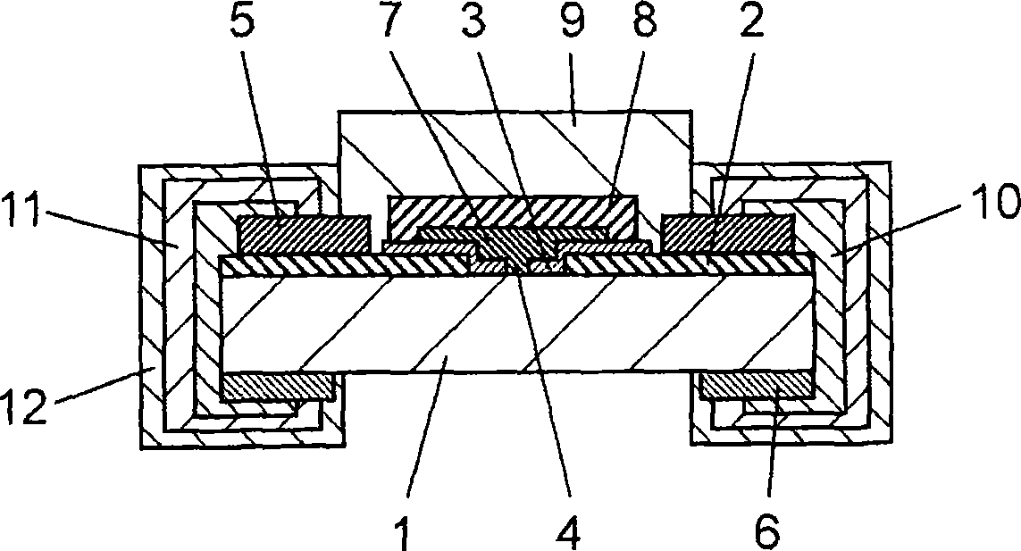
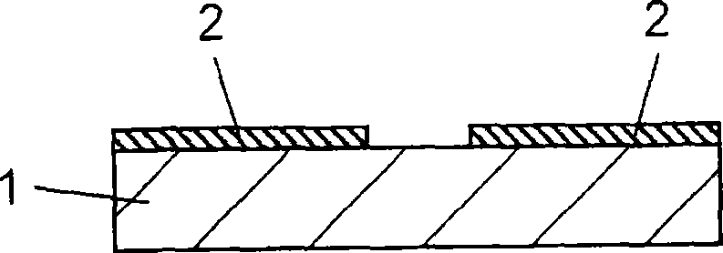
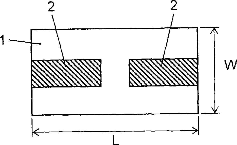
[0046] Next, using the first embodiment, refer to the appended Figure 1 Next, the antistatic component and its manufacturing method will be described. figure 1 It is a drawing showing a sectional view of the antistatic member according to the first embodiment of the present invention. Such as figure 1As shown, the antistatic component according to the first embodiment of the present invention has a pair of first electrodes 2, and the pair of first electrodes 2 are formed on the upper surface of the alumina substrate 1, which is an insulating substrate with a relative dielectric constant of 50 or less, preferably 10 or less. The top constitutes the extraction electrode. The second electrode 3 is located between the pair of first electrodes 2 and partially overlaps with the first electrodes 2 and is electrically connected. The second electrode 3 is made of a material with a high melting point, and has a thinner film thickness than the first electrode 2 . A gap 4 provided by...
no. 2 approach
[0077] Below, while referring to the attached Figure 1 The antistatic member of the second embodiment and its manufacturing method will be described. In the antistatic member according to the second embodiment of the present invention, the second electrode 3 is formed of a material mainly composed of nickel. Except for this point, it is the same structure as the above-mentioned first embodiment of the present invention. Therefore, its cross-section is the same as figure 1 In addition, the manufacturing process diagram showing its manufacturing method is also the same as Figure 2A ~ Figure 7B same. Furthermore, its electrostatic test method is the same as that of the first embodiment by using Figure 8 method is carried out. Since they are the same, descriptions of the cross-sectional views, manufacturing process drawings, and electrostatic test methods are omitted.
[0078] In the antistatic component of the second embodiment of the present invention constituted as abo...
no. 3 approach
[0091] Next, using the third embodiment, while referring to the attached Figure 1 Next, the antistatic component and its manufacturing method will be described.
[0092]The antistatic member according to the third embodiment of the present invention comprises the second electrode 3 from a material mainly composed of aluminum. Except for this point, the rest is the same structure as the above-mentioned first embodiment of the present invention, therefore, its cross-sectional view is the same as figure 1 In addition, the manufacturing process diagram showing its manufacturing method is also the same as Figure 2A ~ Figure 7B The same, and its electrostatic test method is also the same as Figure 8 Same as explained. Therefore, descriptions of the cross-sectional views, manufacturing process drawings, and electrostatic test methods are omitted.
[0093] In the antistatic component of the third embodiment of the present invention constituted as above, the results of the stati...
PUM
| Property | Measurement | Unit |
|---|---|---|
| Resistivity | aaaaa | aaaaa |
| Film thickness | aaaaa | aaaaa |
| Film thickness | aaaaa | aaaaa |
Abstract
Description
Claims
Application Information
 - R&D Engineer
- R&D Manager
- IP Professional
- Industry Leading Data Capabilities
- Powerful AI technology
- Patent DNA Extraction
Browse by: Latest US Patents, China's latest patents, Technical Efficacy Thesaurus, Application Domain, Technology Topic.
© 2024 PatSnap. All rights reserved.Legal|Privacy policy|Modern Slavery Act Transparency Statement|Sitemap