
Method for preparing iron silicide nano wires

A nanowire, iron silicide technology, applied in nanostructure manufacturing, chemical instruments and methods, nanotechnology and other directions, can solve problems such as limiting the scope of application, not conducive to energy saving and large-scale production, to expand the scope of application and achieve large-scale production. Production, energy saving effect

Active Publication Date: 2009-10-07
TSINGHUA UNIV +1
View PDF0 Cites 3 Cited by
  • Summary
  • Abstract
  • Description
  • Claims
  • Application Information

AI Technical Summary

Problems solved by technology

Therefore, it is not conducive to saving energy and mass production
Secondly, this method can only grow iron silicide nanowires on silicon wafers, which limits its application range.

Method used


Image

  • Method for preparing iron silicide nano wires
  • Method for preparing iron silicide nano wires
  • Method for preparing iron silicide nano wires

Examples


Embodiment Construction

[0015] The technical solution will be further described in detail below in conjunction with the accompanying drawings.

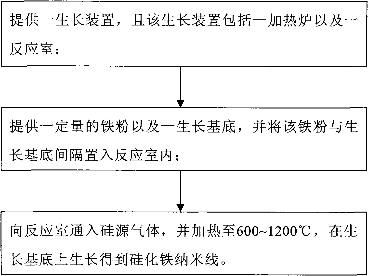
[0016] see figure 1 and figure 2 The embodiment of the technical solution provides a method for preparing iron silicide nanowires, which specifically includes the following steps:

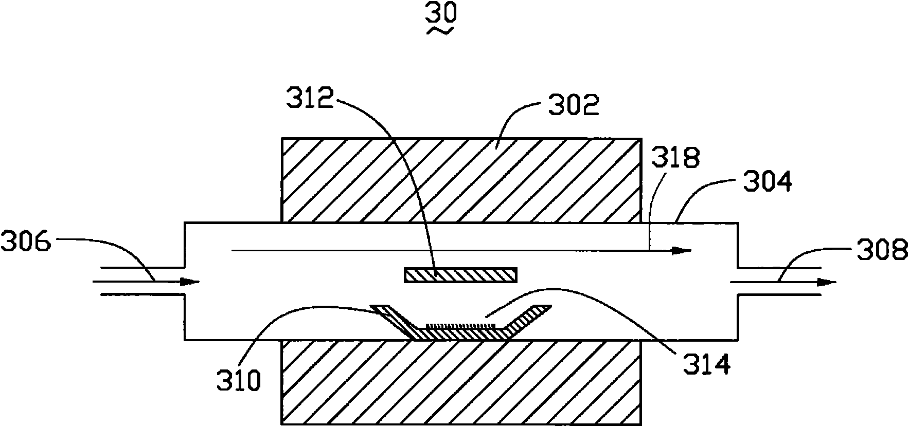
[0017] In step 1, a growth device 30 is provided, and the growth device 30 includes a heating furnace 302 and a reaction chamber 304 .

[0018] In this embodiment, the reaction chamber 304 is preferably a quartz tube with a gas inlet 306 and a gas outlet 308 at both ends thereof. The quartz tube is movable in the heating furnace 302, and its length is longer than the heating furnace 302, so that when the quartz tube is pushed and pulled in the experiment, a part of the quartz tube can always be placed in the heating furnace 302.

[0019] The reaction chamber 304 also includes a carrying device 310 which is a container with a high melting point. In this embodiment, the suppor...


PUM

PropertyMeasurementUnit
diameteraaaaaaaaaa
lengthaaaaaaaaaa
boiling pointaaaaaaaaaa

Abstract

The invention relates to a method for preparing iron silicide nano wires, which particularly comprises the following steps: a growing device is provided and comprises a heating furnace and a reaction chamber, a certain amount of iron powder and a growing base are provided and are arranged in the reaction chamber at intervals, silicon source gas is charged into the reaction chamber, the reaction chamber is heated to be 600-1200 DEG C, and the iron silicide nano wires are obtained by growing on the growing base.

Description

technical field [0001] The invention relates to a method for preparing nanometer materials, in particular to a method for preparing iron silicide nanowires. Background technique [0002] The direction of development of the semiconductor industry is smaller, faster, and lower energy consumption. However, after entering the era of nanoelectronics from the era of microelectronics, the traditional semiconductor manufacturing technology - photolithography ("top-down" technology) is becoming more and more difficult to meet the current and future requirements. Therefore, "bottom-up" technology, or self-assembly technology is considered to be the trend of future development. At present, people have used this self-assembly technology to synthesize various nanostructures, including nanowires and nanotubes, and their potential applications include nanoelectronics, nanooptics, and nanosensors. [0003] Iron silicide nanowires (FeSi nanowires) are a narrow bandgap semiconductor with un...

Claims


Application Information

Patent Timeline
Patent Type & Authority Applications(China)
IPC IPC(8): C01B33/06B82B3/00
CPCC01B33/06Y10S117/902
Inventor 孙海林姜开利李群庆范守善
Owner TSINGHUA UNIV
Learn More