A device modeling method in relation to total dose radiation

A technology of total dose radiation and device modeling, applied in instruments, special data processing applications, electrical digital data processing, etc., to achieve the effects of increasing fitting accuracy, improving accuracy, improving design efficiency and success rate

Inactive Publication Date: 2009-10-07
BEIJING MXTRONICS CORP +1
View PDF0 Cites 25 Cited by
  • Summary
  • Abstract
  • Description
  • Claims
  • Application Information

AI Technical Summary

Problems solved by technology

[0005] The technical problem of the present invention is: to overcome the deficiencies of the prior art, to provide a device modeling method related to the total dose radiation, to solve

Method used


Image

  • A device modeling method in relation to total dose radiation
  • A device modeling method in relation to total dose radiation
  • A device modeling method in relation to total dose radiation

Examples


Embodiment Construction

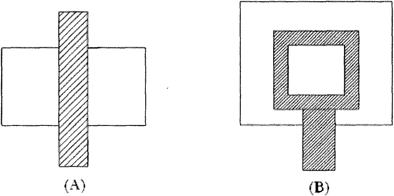
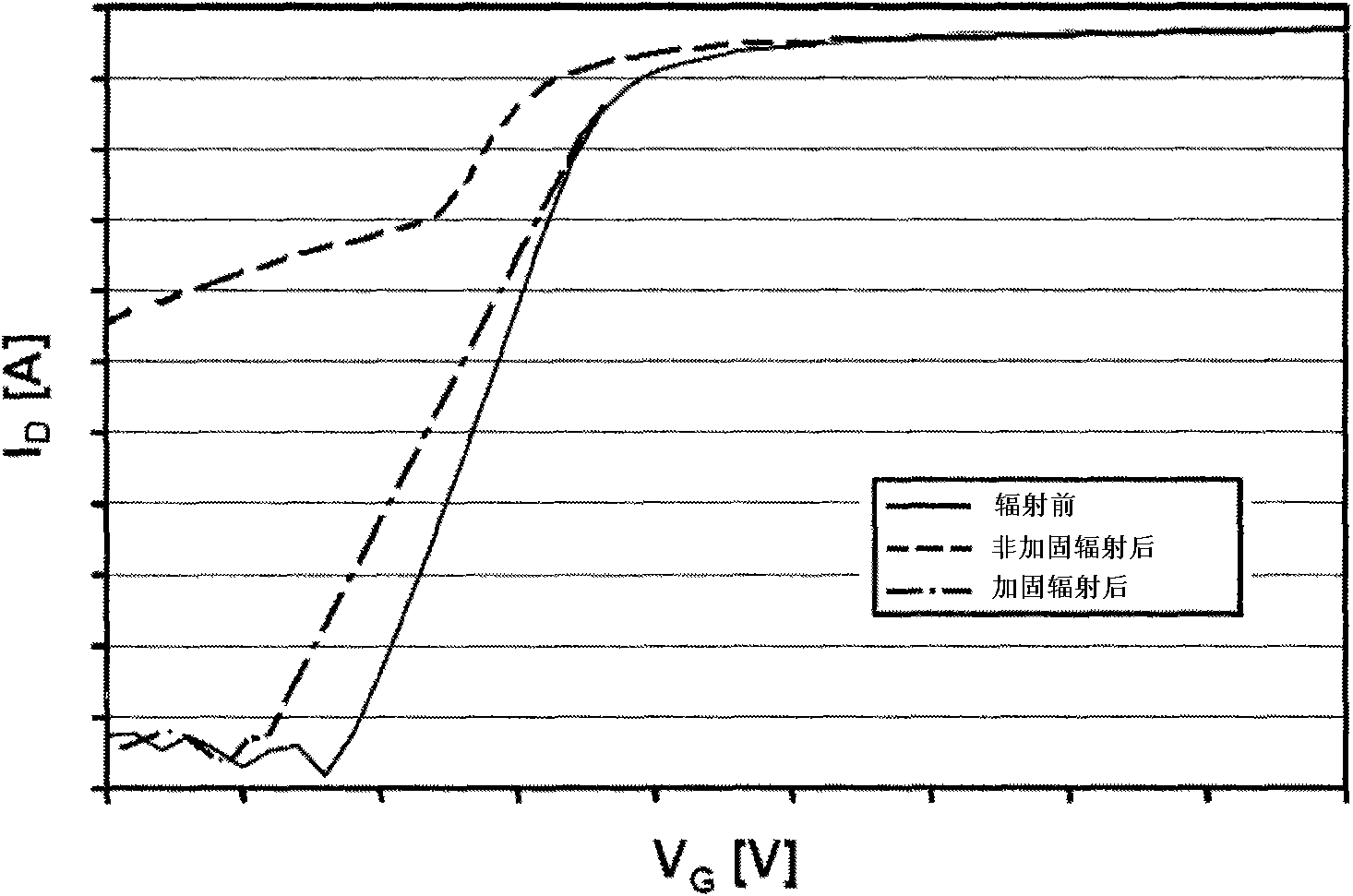
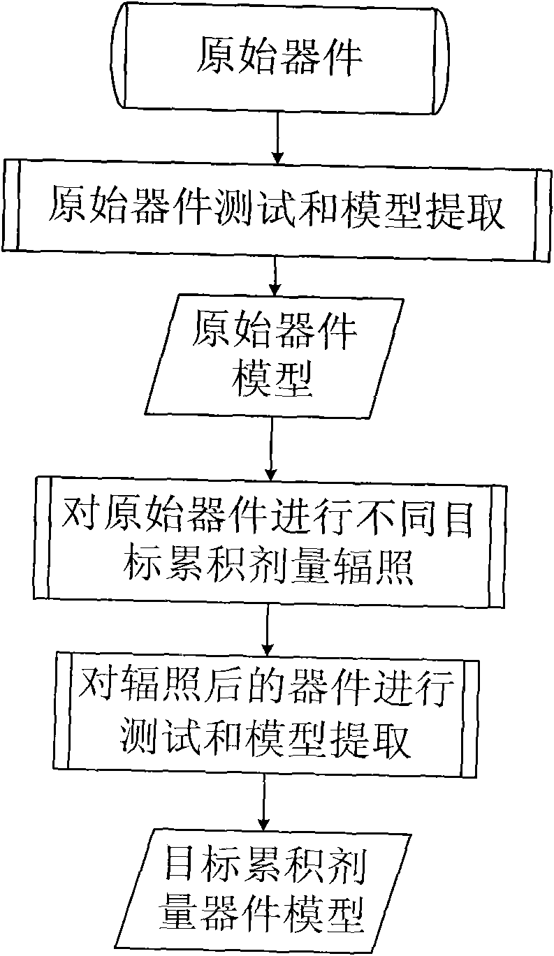
[0017] The method of the present invention is applicable to both hardened and non-hardened devices, where the devices can be active devices, such as transistors, or passive devices, such as capacitors and resistors. Combine below image 3 The flow chart shown uses a non-reinforced transistor as an example to illustrate the specific implementation process of the present invention. First, in order to model, design and manufacture an original electronic device, such as non-reinforced transistors. In order to achieve higher modeling accuracy, each set of transistors is designed with 8 types of lengths and 8 types of widths, a total of 64 of the same type and different sizes. Devices, use layout design tools to design the layout of each device, and lead out each electrode of each device for testing and experimentation. The 64 original devices were tested respectively, and the current-voltage (IV) characteristics and capacitance-voltage (CV) characteristics of the 64 original devic...


PUM


Abstract

A device modeling method in relation to total dose radiation, wherein firstly, an original electronic device is designed and undergoes testing and model extraction to obtain the model of the original device, secondly, the obtained original device undergoes radiation at different target cumulative doses and model extraction to obtain the device model after radiation at all target cumulative doses, and lastly, the obtained original device model and the device model that has received radiation at all target cumulative doses jointly constitute the device model in relation to total dose radiation. Through testing and parameter extraction of the original device and the device that has received radiation at all target cumulative doses, the present invention provides a method for accurate modeling of hardened devices and unhardened devices. Meanwhile it adds radiation dose as a variable into the realization method of device model so that the performance of the circuit that has received radiation at different doses can be accurately predicted through simulation, thus raising the design efficiency and success rate of the circuits.

Description

technical field [0001] The invention relates to a device modeling method, in particular to a device modeling method related to total dose radiation. Background technique [0002] When designing an integrated circuit, it is usually necessary to simulate the designed circuit structure in order to have a certain estimate of the function and performance of the circuit before the circuit is manufactured. The device model used in simulation directly affects the accuracy of simulation. The so-called device model is a collection of a series of electrical parameters and physical parameters, using these simplified abstract parameters to simulate the characteristics of complex real devices. A good device model is a key factor to ensure the success of circuit design. [0003] The total dose effect refers to the phenomenon that oxide trap charges and interface state charges are accumulated in the insulating layer (mainly the oxide layer) when the semiconductor device is exposed to radi...

Claims


Application Information

Patent Timeline
IPC IPC(8): G06F17/50
Inventor 王亮岳素格孙永姝
Owner BEIJING MXTRONICS CORP
Why Eureka
Try Eureka