Array package substrate

An array packaging and substrate technology, applied in electrical components, electrical solid devices, circuits, etc., can solve problems such as solder balls falling off easily

Inactive Publication Date: 2009-10-07
SUBTRON TECH
View PDF0 Cites 6 Cited by
  • Summary
  • Abstract
  • Description
  • Claims
  • Application Information

AI Technical Summary

Problems solved by technology

[0006] The invention provides an array packaging substrate, whi

Method used


Image

  • Array package substrate
  • Array package substrate

Examples


Embodiment Construction

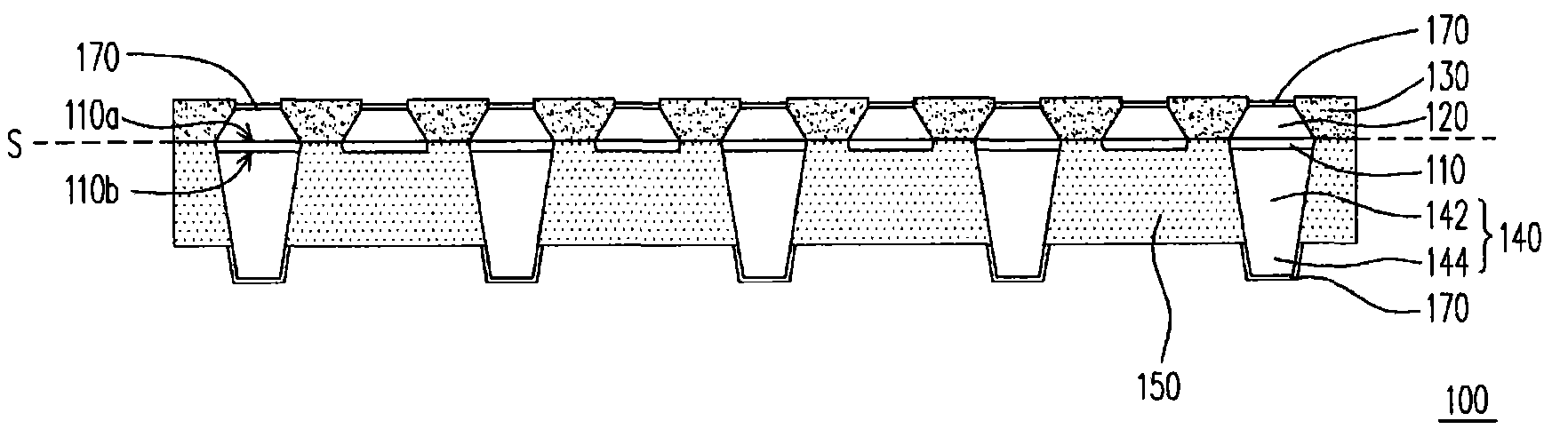
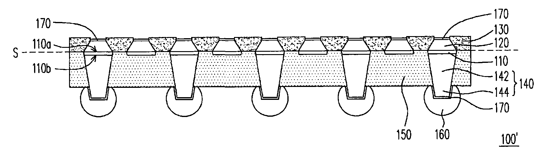
[0026] figure 1 A schematic diagram of an array packaging substrate according to an embodiment of the present invention is shown. Please refer to figure 1 , the array package substrate 100 of this embodiment is used to carry a semiconductor element such as a chip. The array package substrate 100 mainly includes a patterned metal connection layer 110 (patterned metal connection layer 110 is an etch barrier layer) made of nickel or nickel chrome, a plurality of pads 120 made of copper, a first The insulating layer 130 , a plurality of conductive studs 140 made of copper, for example, and the second insulating layer 150 . In this embodiment, the patterned metal connection layer 110 has a first surface 110a and a second surface 110b corresponding to the first surface 110a, the pads 120 are disposed on the first surface 110a, and the conductive bumps The post 140 is disposed on the second surface 110b. In this way, the conductive bumps 140 can be electrically connected to the p...


PUM


Abstract

The invention discloses an array package substrate which comprises a patterning metal connecting layer, a plurality of connecting gaskets, a first insulation layer, a plurality of conductive projections and a second insulation layer. The patterning metal connecting layer is provided with a first surface and a second surface which corresponds to the first surface, the connecting gaskets are arranged on the first surface, the conductive projections are arranged on the second surface and are electrically connected with the connecting gaskets through the patterning metal connecting layer, wherein each conductive projection is provided with a connecting part and a projection part, and the connecting part of each conductive projection is connected with the patterning metal connecting layer. In addition, the first insulation layer is arranged at one side of the surface planar with the first surface or second surface and protrudes from the connecting gaskets. The second insulation layer is arranged at the other side of the surface and protrudes from the projection part of each conductive projection.

Description

technical field [0001] The present invention relates to an array package substrate, and in particular to a ball grid array (BGA) package substrate. Background technique [0002] In recent years, with the rapid development of electronic technology and the emergence of high-tech electronic industries, electronic products with more humanization and better functions are constantly being introduced, and are designed towards the trend of light, thin, short and small. At present, in the semiconductor packaging process, array packaging substrates are one of the commonly used packaging components, and semiconductor components (such as chips) can be correspondingly located on each array substrate. After the semiconductor elements are electrically connected to the array substrates, all the semiconductor elements in each array substrate are covered with a molding compound to form an array package type chip package structure. Finally, each array substrate and its corresponding encapsula...

Claims


Application Information

Patent Timeline
IPC IPC(8): H01L23/498
Inventor 吴建男李胜雄杨耿忠
Owner SUBTRON TECH
Why Eureka
Try Eureka