Wafer-level packaging of chip and packaging method thereof

A wafer-level packaging and packaging method technology, applied in electrical components, electrical solid-state devices, circuits, etc., can solve the problems affecting the bonding quality of the whole chip, the decline in yield, and the inability to achieve sealing.

Active Publication Date: 2009-10-07
THE 13TH RES INST OF CHINA ELECTRONICS TECH GRP CORP
View PDF4 Cites 32 Cited by
  • Summary
  • Abstract
  • Description
  • Claims
  • Application Information

AI Technical Summary

Problems solved by technology

However, the current bonding rings are all flat and have no structure, so the requirements for the surface and equipment are very high. The stress in the whole piece will greatly affect the bonding quality of the whole piece.

Method used


Image

  • Wafer-level packaging of chip and packaging method thereof
  • Wafer-level packaging of chip and packaging method thereof
  • Wafer-level packaging of chip and packaging method thereof

Examples


Embodiment 1

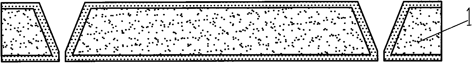
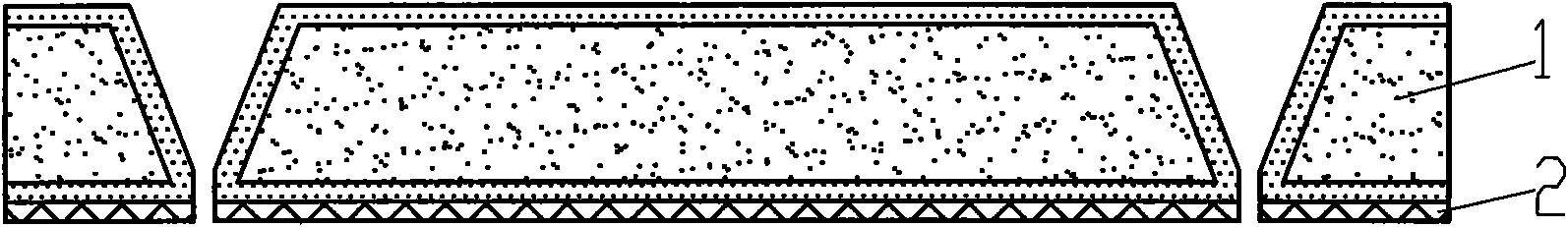
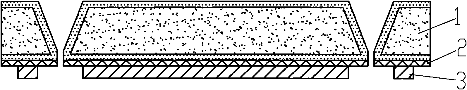
[0048] Example 1: Figure 3-2 As shown, the wafer-level package of the chip is packaged by an upper cover wafer and a lower cover wafer made of silicon wafers. There is an upper sealing ring on the upper cover disc, and a lower sealing ring matching the lower sealing ring on the lower cover disc; the upper sealing ring and the lower sealing ring are eutectic or hot-pressed Implement encapsulation.

[0049] The wafer-level packaging of this chip uses thermocompression bonding of tin-lead and gold for wafer-level packaging. Concrete process steps are as follows:

[0050] 1. Preparation of the upper cover wafer: prepare the upper cover wafer 1 with or without through holes having the same size as the wafer to be packaged. The material of the top cover wafer can be silicon wafer, glass wafer or ceramic wafer, etc. There is no limit to the way of realizing the through hole, and it can be etching, laser drilling, frosting and other means. In this embodiment, a silicon wafer with...

Embodiment 2

[0064] Example 2: Figure 5-2 As shown, the wafer-level package of the chip is packaged by an upper cover wafer and a lower cover wafer made of silicon wafers. A bonding layer of BCB material is coated on the upper cover disc, and a lower sealing ring matching the lower sealing ring is provided on the lower cover disc; the lower sealing ring is extruded to the bonding layer to realize packaging.

[0065] The wafer-level packaging of this chip uses cold-compression bonding of BCB and gold for wafer-level packaging. The specific process steps are as follows:

[0066] 1. Preparation of the top cover wafer: prepare a top cover wafer with or without through holes of the same size as the wafer to be packaged. The material of the top cover wafer can be silicon wafer, glass wafer or ceramic wafer, etc. There is no limit to the way of realizing the through hole, and it can be etching, laser drilling, frosting and other means. In this embodiment, a silicon wafer with a thickness of 3 ...


PUM


Abstract

The present invention discloses a wafer-level packaging of chip and a packaging method thereof. The wafer of upper cover plate is installed with an upper sealing ring strip. The wafer of lower cover plate is installed with a lower sealing ring strip matched with the lower sealing ring strip. The upper sealing ring strip and the lower sealing ring strip are eutectic or hot-pressed and spread for realizing packaging. Or the wafer of upper cover plate is coated with a bonding layer of epoxy resin, polymer, metal or alloy material. The wafer of lower cover plate is installed with a lower sealing ring strip matched with the upper sealing ring strip. The lower sealing ring strip squeezes the bonding layer for realizing packaging. The wafer-level packaging of chip can increase the sealing performance of internal and external environments. The packaging period can greatly increase the finished product rate after bonding, increase the sealing quality and guarantees the long-time reliability.

Description

technical field [0001] The invention relates to the technical field of MEMS and microelectronics technology manufacturing, in particular to a chip wafer-level package and a package method thereof. Background technique [0002] With the demand and development of applications, various electronic systems, whether military or civilian, are required to be lightweight, small in size and multifunctional. However, to achieve smaller volume and higher packaging density through the currently widely used tube shell and flip-chip packaging technologies has encountered huge technical and cost challenges. At present, we are going through such a period that the above problems are solved by using the wafer-level packaging process WLP. It can be extended on this technology, and then developed into three-dimensional stacking of different types of chips to achieve the highest packaging density. [0003] Wafer-level packaging technology, as such a key basic manufacturing technology, was origi...

Claims


Application Information

Patent Timeline
IPC IPC(8): H01L25/00H01L23/31H01L21/50H01L21/56H01L21/60
Inventor 何洪涛徐永青
Owner THE 13TH RES INST OF CHINA ELECTRONICS TECH GRP CORP
Why Eureka
Try Eureka