Shifter register for low power consumption application
A shift register, signal technology, used in static memory, digital memory information, instruments, etc.
- Summary
- Abstract
- Description
- Claims
- Application Information
AI Technical Summary
Problems solved by technology
Method used
Image
Examples
Embodiment Construction
[0029] The description of the embodiment of the present invention follows.
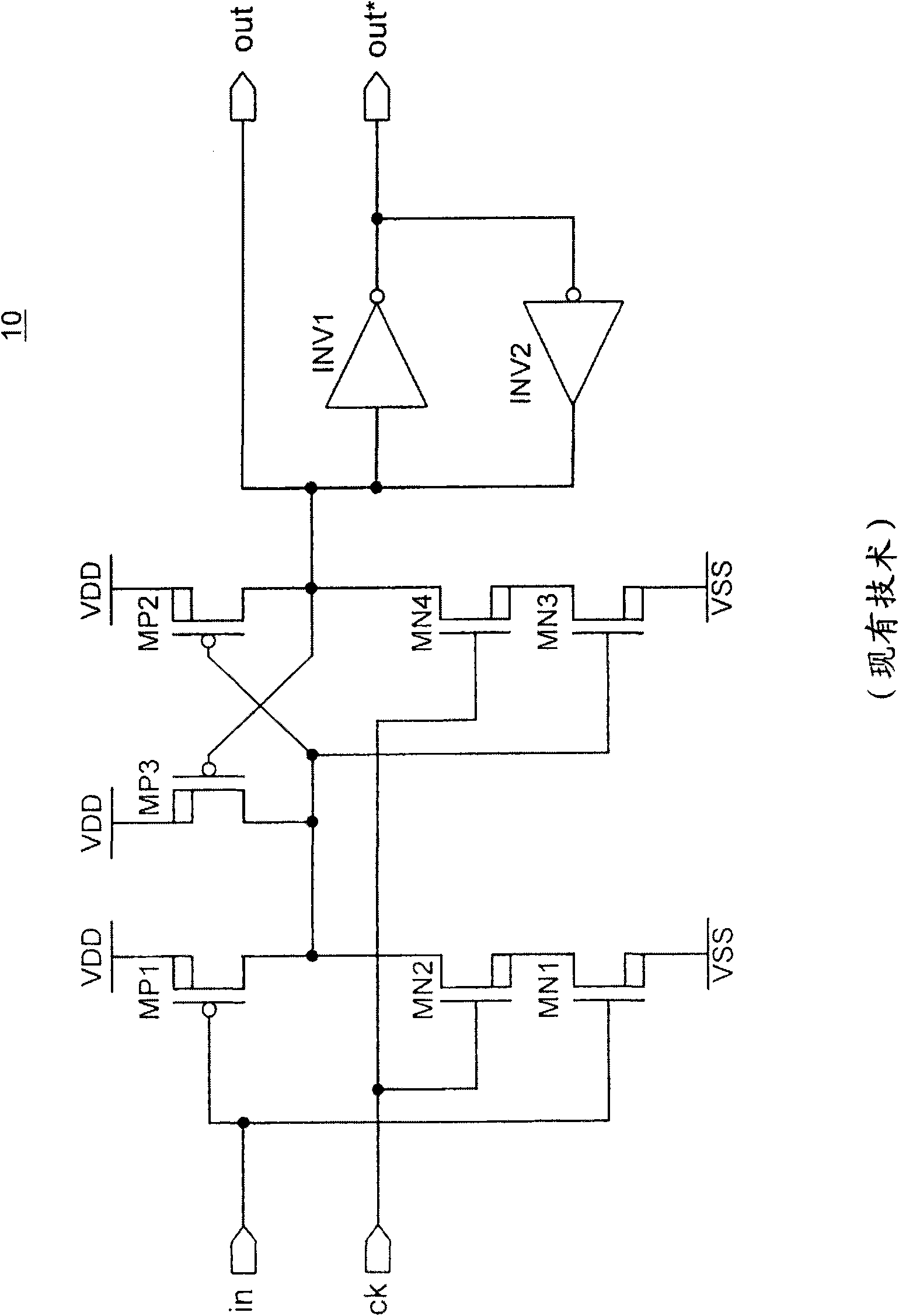
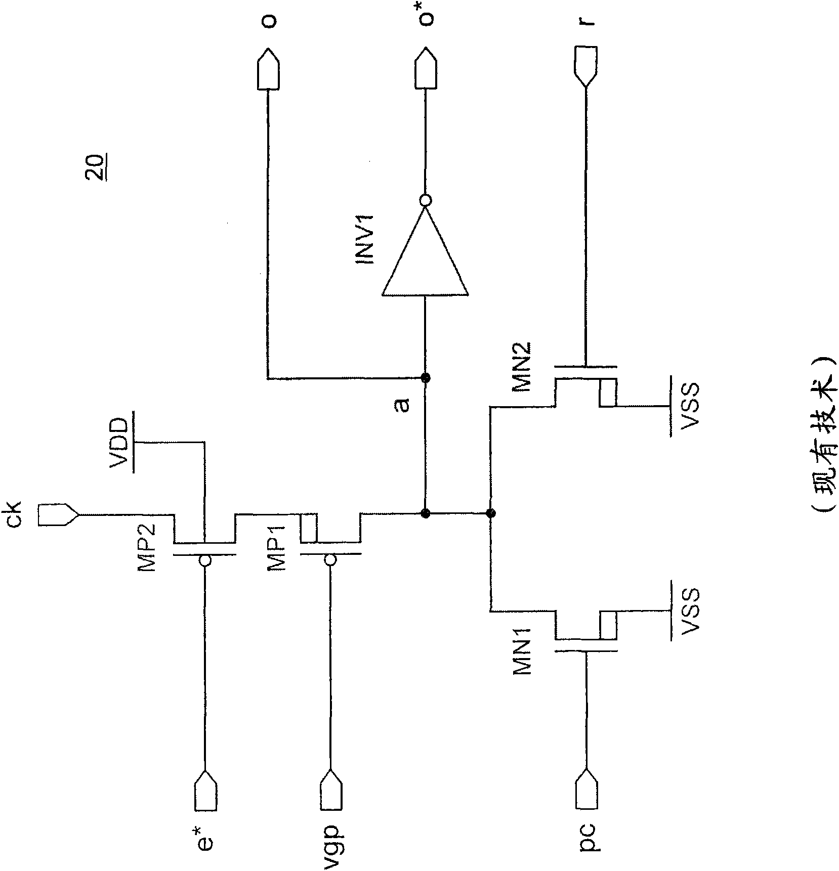
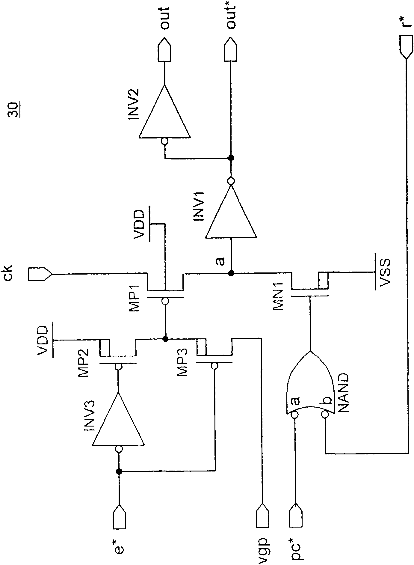
[0030] image 3 explain its improvement in figure 1 and 2 configuration of a circuit 30. Here, the clock signal input ck also drives the primary transistor MP1. However, the gate of MP1 is fed from a pair of cascode transistors MP2 and MP3, which are set at the state of node a as determined by input e * Determined with vgp. From the inverting input e of the previous stage * Feeds to the input terminal of inverter INV3 to control the gate of transistor MP3. The MP3 drain terminal controls the gate of transistor MP1. The source terminal of transistor MP2 is fed from voltage VDD.
[0031] An intentional precharge input pc * together with a reset signal r * for feeding through a single NAND gate. The output of a single NAND gate drives the signal to the gate terminal of buffer transistor MN1. The first inverter INV1 and the second inverter INV2 respectively provide inverted outputs out * and ...
PUM
 Abstract
Description
Claims
Application Information


