Defect detection system of panel component
A defect detection and component technology, used in measuring devices, material analysis by optical means, instruments, etc., can solve problems such as limited adjustment range, attenuation of light intensity, thickness and bulk of light boxes
- Summary
- Abstract
- Description
- Claims
- Application Information
AI Technical Summary
Problems solved by technology
Method used
Image
Examples
Embodiment Construction
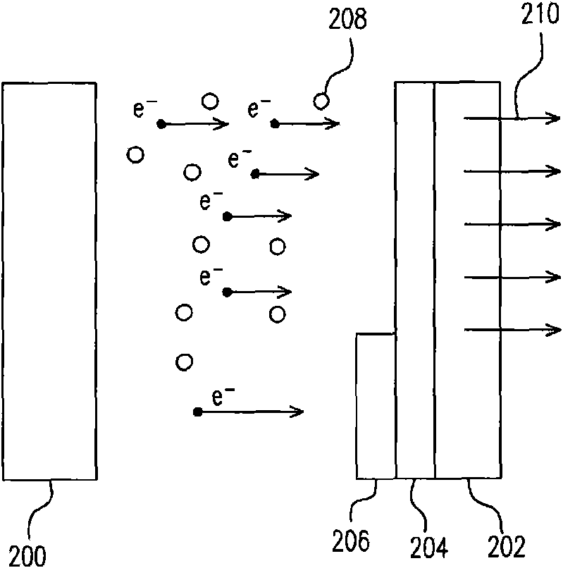
[0033] For example, the present invention can be applied to the product inspection planar light source equipment required on the production line. For the light source part of the detection light box, the present invention proposes an electron emission type flat light source (Flat electron emission lamp, FEEL) as the detection light source. Here, the planar light source refers to a planar light source, which can be a curved surface or a planar surface as required.
[0034] The light source of the detection light box is changed to an electron-emitting planar light source. Because it is a planar light source, there is no need to use a diffuser, which can reduce light loss. In addition, the light source device of the present invention can be manufactured into light sources of different sizes and shapes as required, for example, rectangular or circular as shown in FIG. 8 . The reflective mechanism only needs a flat reflective surface, and the overall detection equipment can be thi...
PUM
 Abstract
Description
Claims
Application Information


