Eureka AIR delivers breakthrough ideas for toughest innovation challenges, trusted by R&D personnel around the world.

Encapsulating method of image sensor

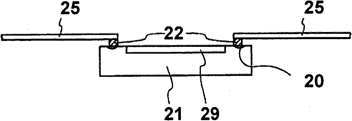
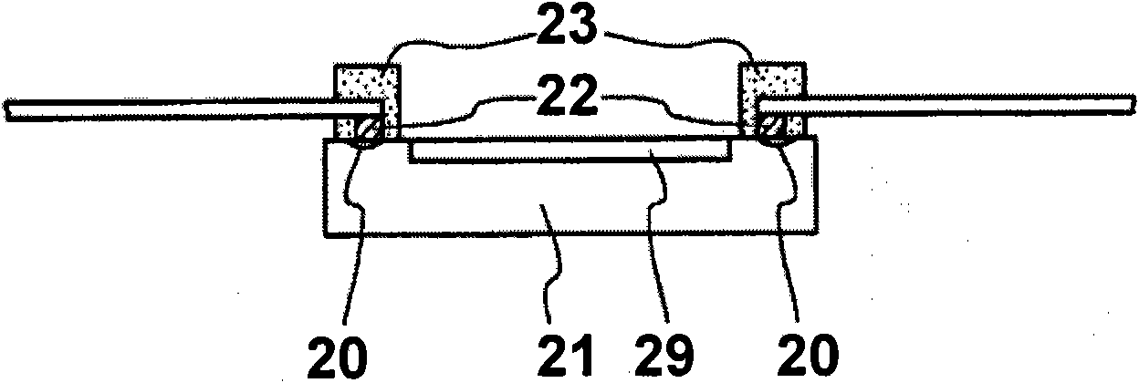
A packaging method and image sensing technology, applied in radiation control devices, electrical components, electrical solid devices, etc., can solve the problems of light refraction, parallel surface of transparent cover electronic devices, and lenses that cannot be parallel.

Inactive Publication Date: 2009-10-28
IMPAC TECH
View PDF3 Cites 5 Cited by
  • Summary
  • Abstract
  • Description
  • Claims
  • Application Information

AI Technical Summary

Problems solved by technology

However, the molding process disclosed in the prior art can damage at least one of the mutual electrical connections and the surface of the central exposed area of ​​the electronic device
Without further flattening the molded barrier, the transparent cover cannot be parallel to the surface of the electronic device, so light will be refracted when passing through the transparent cover
[0009] Although the prior art mentioned above is technically feasible, it is difficult to realize in practice
Existing molding processes can damage the bonding wires and the central exposed area of ​​the image sensing device
On the other hand, the lens may not be parallel to the surface of the image sensing device, so when light passes through the lens, it will cause light refraction

Method used


Image

  • Encapsulating method of image sensor
  • Encapsulating method of image sensor
  • Encapsulating method of image sensor

Examples


Embodiment Construction

[0043] Figures 4A to 4I An embodiment of the packaging method of the image sensing device of the present invention is shown. First, please refer to Figure 4A . A substrate 41 is provided which may be made of plastic, glass fiber reinforced epoxy resin or bismaleimide triazine resin. In addition, the substrate 41 can be made of aluminum nitride ceramics to improve thermal conductivity. like Figure 4B As shown, the image sensing module 42 mounted on the substrate 41 has an exposed light receiving area 421 . Traditionally, the image sensing module 42 is mounted on the substrate 41 using a tape lamination process. In this embodiment, the image sensing module 42 is mounted on the substrate 41 through the adhesive layer 411 . Generally, many connection pads (not shown in the figure) are arranged on the image sensing module 42 and the substrate 41 . The connection pads of the image sensing module 42 and the substrate 41 are conducted via a plurality of bonding wires 43, such...


PUM


Abstract

The invention discloses an encapsulating method of an image sensor, which comprises the following steps: an image sensing module with an exposed light receiving area is arranged on a base plate; the image sensing module and the base plate are connected by a plurality of bonding wires; a protecting layer is formed on the light receiving area of the image sensing module; moulding layer is formed to seal the bonding wires; the protecting layer and the moulding layer are flattened; the protecting layer is removed to expose the light receiving area of the image sensing module; and a transparent lid base is formed.

Description

technical field [0001] The present invention relates to a semiconductor packaging method, in particular to a packaging method for an image sensing device. Background technique [0002] In recent years, solid-state image sensors such as charge-coupled device (CCD) image sensors or complementary metal-oxide-semiconductor (CMOS) image sensors have been widely used in electronic products to convert light into electrical signals. Applications of image sensor components include displays, mobile phones, transcription machines, scanners, digital cameras, etc. [0003] Traditionally, sensors are mounted on a substrate and enclosed in a housing assembly ready for packaging. The housing assembly includes a transparent cover to allow the sensor to receive light or other forms of radiation. The cover can be a flat window or be lens-shaped to provide optical properties. The base plate and the shell are usually made of ceramic materials, and the cover is glass or a nearly transparent su...

Claims


Application Information

Patent Timeline
IPC IPC(8): H01L21/50H01L21/60H01L21/56H01L27/146
CPCH01L2224/48091
Inventor 黄吉志许志扬
Owner IMPAC TECH
Why Eureka
Eureka Blog
Learn More