

Semiconductor device and method for manufacturing the same
一种制造方法、半导体的技术,应用在半导体/固态器件制造、半导体器件、晶体管等方向,能够解决产生凸起状特性等问题,达到降低凸起状特性、实现功耗的效果
- Summary
- Abstract
- Description
- Claims
- Application Information
AI Technical Summary
Problems solved by technology
Method used
Image

Examples
Embodiment approach 1
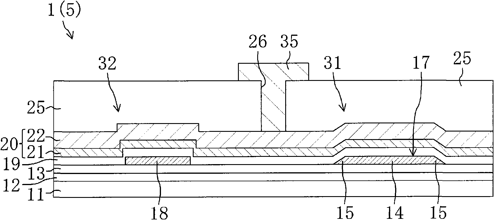
[0054] Figure 1 to Figure 12 Embodiment 1 of this invention is shown.
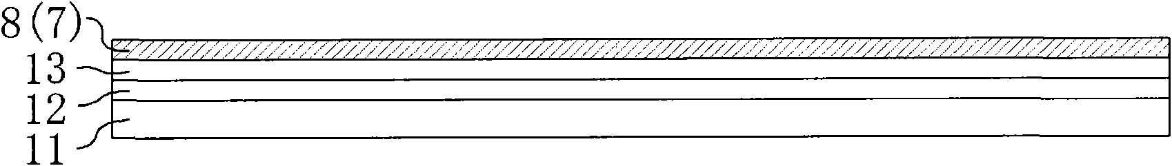
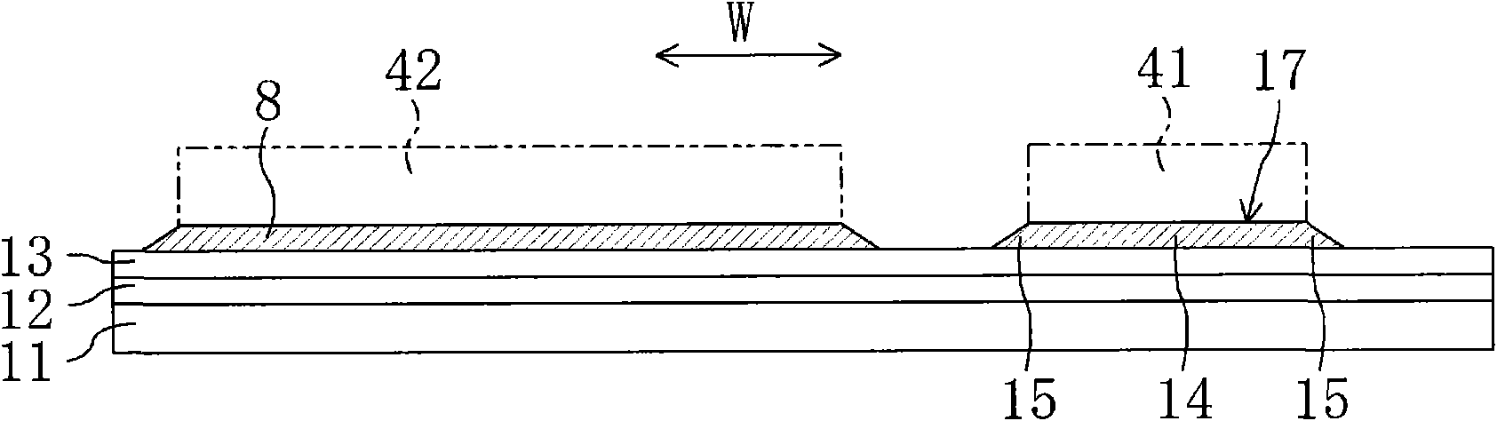
[0055] Figure 9 It is a plan view showing main parts of the semiconductor device 1 of the first embodiment. figure 1 Yes Figure 9 I-I line sectional view. Figure 2 to Figure 8 It is a sectional view showing each manufacturing process of the semiconductor device 1 . Figure 10 It is a graph showing the current-voltage characteristic of the semiconductor device 1 . Figure 11 is a cross-sectional view showing a schematic configuration of the liquid crystal display device S. FIG. Figure 12 It is a cross-sectional view schematically showing a first semiconductor layer 17 and a second semiconductor layer 18 which will be described later.
[0056] The semiconductor device 1 of this embodiment constitutes the active matrix substrate 10 of the liquid crystal display device S, for example. First, the schematic configuration of the liquid crystal display device S will be described.
[0057] like Figu...
Embodiment approach
[0129] In Embodiment 1 above, the semiconductor device 1 was used as an example to describe the active matrix substrate 10 constituting the liquid crystal display device S and on which the drive circuit 5 is formed. Active matrix substrates for other display devices such as devices. In addition, any semiconductor device including p-type TFTs and n-type TFTs can be similarly applied.
PUM
 Abstract
Description
Claims
Application Information