Electrode structure of smectic LCD baseplate and manufacturing method thereof

A technology of liquid crystal display and electrode structure, which is applied in the photographic process of pattern surface, semiconductor/solid-state device manufacturing, circuit, etc., and can solve the problems of large non-effective electrode area, poor display effect, and low resolution. Achieve the effects of compact electrode structure, saving process and cost, and reducing area

Inactive Publication Date: 2009-11-11
HALATION PHOTONICS CORP
View PDF0 Cites 4 Cited by
  • Summary
  • Abstract
  • Description
  • Claims
  • Application Information

AI Technical Summary

Problems solved by technology

However, this traditional electrode structure using a passive driving method is only suitable for small screens with low resolution and small pixel area, and since this electrode structure needs to leave enough space outside its effective electrode area to set The area where the upper and lower substrate electrodes are connected and the wiring, so the area of ​​the non-effective electrode area of ​​this electrode structure is very large, and multiple display screens cannot be spliced ​​very tightly, and the display effect after splicing is poor.

Method used


Image

  • Electrode structure of smectic LCD baseplate and manufacturing method thereof
  • Electrode structure of smectic LCD baseplate and manufacturing method thereof
  • Electrode structure of smectic LCD baseplate and manufacturing method thereof

Examples


Embodiment Construction

[0026] The present invention will be described in further detail below in conjunction with the accompanying drawings.

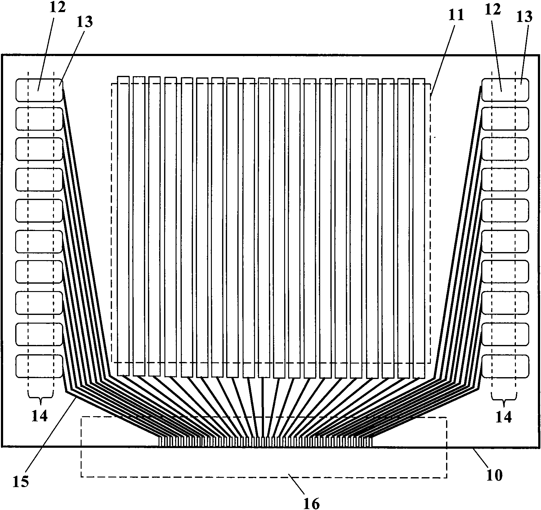
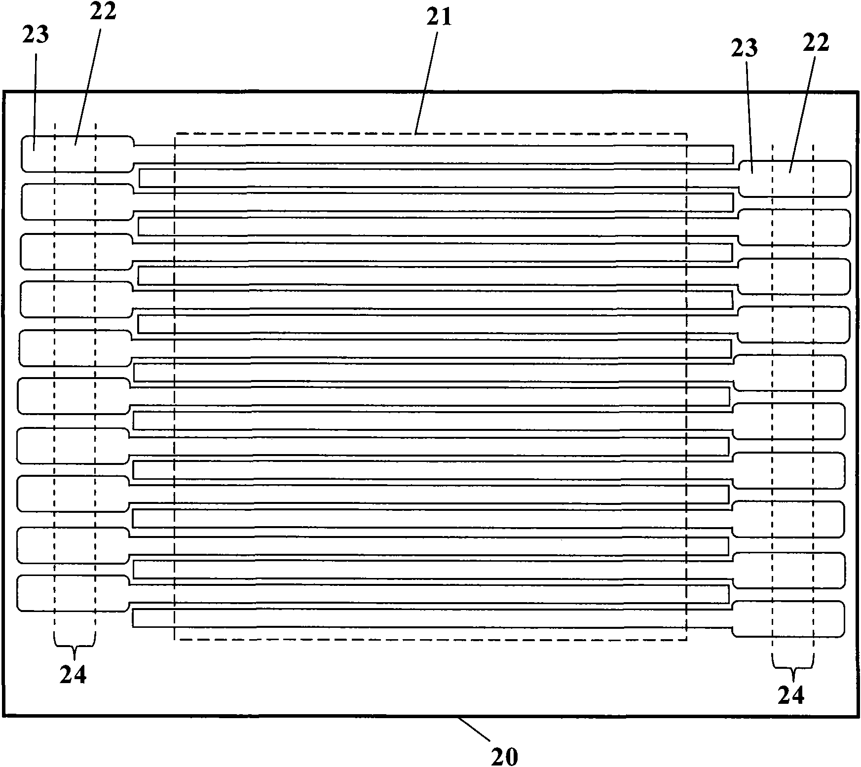
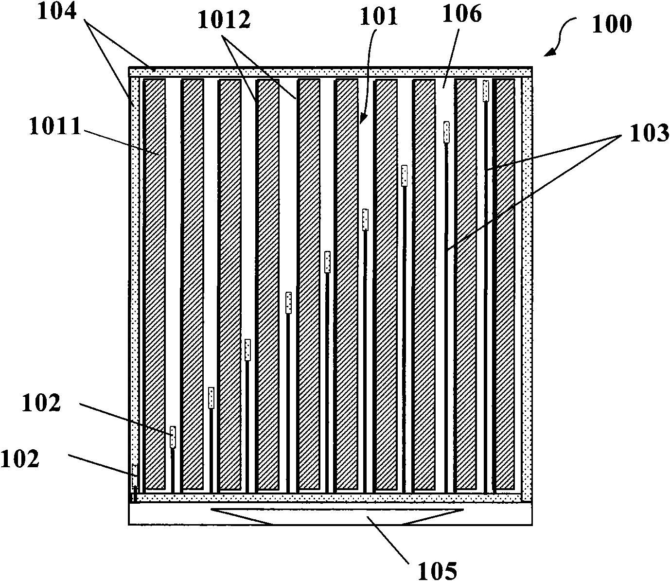
[0027] Such as image 3 and Figure 4 As shown, the electrode structure of the present invention is suitable for liquid crystal display substrates such as substrates of smectic liquid crystal displays with large pixel areas and large gaps between pixels. The smectic liquid crystal display includes an upper substrate and a lower substrate. A mixed layer composed of smectic liquid crystal and additives is arranged between the upper substrate and the lower substrate. An electrode structure is arranged on the side of the upper and lower substrates facing the mixed layer. , the material of the upper and lower substrates can be glass or plastic. The smectic liquid crystal may be a type-A smectic liquid crystal (Smectic-A) organic compound, such as a compound with a siloxy group, tetracyanotetraoctylbiphenyl, decyl tetraacetate tetracyanobiphenyl, and the like. T...


PUM

PropertyMeasurementUnit
thicknessaaaaaaaaaa

Abstract

The invention discloses an electrode structure of a smectic LCD baseplate and a manufacturing method thereof. The electrode structure has the structure that an upper baseplate is provided with strip electrodes consisting of ITO electrodes and strip metal electrodes, wherein each strip electrode is provided with a vertically-conducted metal electrode; a lower baseplate is provided strip electrodes consisting of ITO electrodes and strip metal electrodes, wherein each vertically-conducted connection area is arranged at the clearance beside each strip electrode; and the vertically-conducted metal electrodes of the upper baseplate and the vertically-conducted connection areas of the lower baseplate are arranged correspondingly. The manufacturing method of the electrode structure comprises the following steps: cleaning the baseplates; forming the ITO electrodes; forming metal electrode base courses; and electroplating metal of the top layer to form metal electrodes. The electrode structure manufactured by the manufacturing method is compact, fully takes advantage of effective electrode areas, reduces ineffective electrode areas and can realize continuous splicing of a plurality of LCDs. The electrode structure is suitable for LCDs with larger pixel point areas and larger points among pixels, in particular for smectic LCDs.

Description

technical field [0001] The invention relates to an electrode structure and a manufacturing method thereof, in particular to an electrode structure of a smectic liquid crystal display substrate and a manufacturing method thereof. Background technique [0002] Currently, for a traditional liquid crystal display, there are mainly two driving methods for the electrodes on the display substrate: Active matrix and Passive matrix. [0003] For an electrode structure using an active driving method, a multi-layer thin film process is generally used to realize direct TFT (Thin Film Transistor, thin film transistor) driving of each pixel. At present, traditional liquid crystal displays and liquid crystal TVs with full-color large screens must adopt the electrode structure of this active driving method. However, this electrode structure is expensive, and the initial investment is too much. [0004] The electrode structure is very simple for an electrode structure using a passive drivin...

Claims


Application Information

Patent Timeline
Patent Type & Authority Applications(China)
IPC IPC(8): G02F1/1343G02F1/1333G03F7/00H01L21/00
Inventor 孙刚
Owner HALATION PHOTONICS CORP
Why Eureka
Try Eureka