

Semiconductor detector for measuring radiation and imaging device
A semiconductor and detector technology, applied in the field of semiconductor detectors and imaging devices, can solve the problems that counting multi-energy detection and imaging devices cannot fully meet the requirements of strong X-ray machine radiation, and achieve flexible division methods, improved consistency, The effect of simple structure
- Summary
- Abstract
- Description
- Claims
- Application Information
AI Technical Summary
Problems solved by technology
Method used
Image

Examples
Embodiment Construction
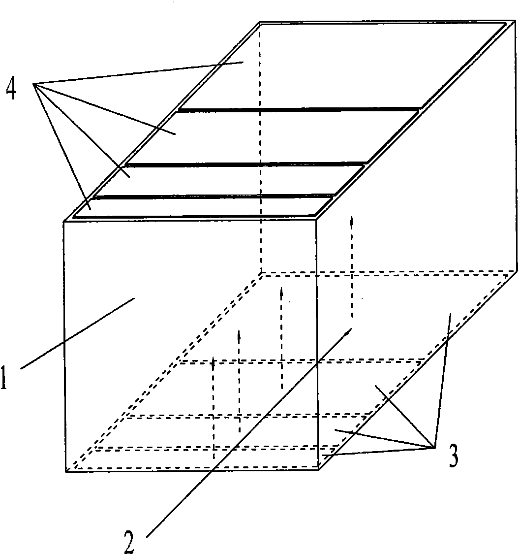
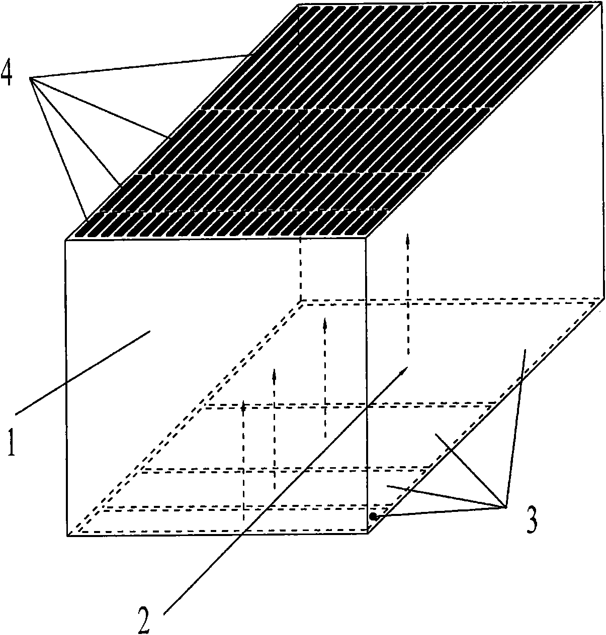
[0029] The principle that the semiconductor detector for measuring radiation of the present invention realizes multi-energy segment detection is that rays of different energies have different penetration distances in the semiconductor medium. In the semiconductor medium, as the ray penetration distance increases, the low-energy ray is absorbed first, and then the high-energy ray is absorbed. Therefore, it can be divided into several sections according to the penetration distance of the ray in the semiconductor medium, and the energy deposition amount of the corresponding energy section is detected in each section.
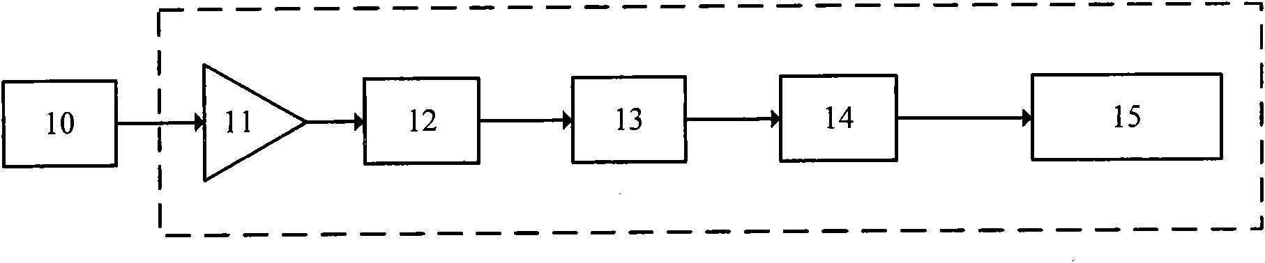
[0030] figure 1 The structure of a semiconductor detector for measuring radiation according to the invention is schematically represented. The measurement signal detected by the sensor 11 is transmitted to a signal processing circuit. The signal processing circuit works according to the current integration mode, including a preamplifier 11 , a main amplifier 12 ,...
PUM
 Abstract
Description
Claims
Application Information