Realization method of tunable superlattice oscillator

An implementation method and superlattice technology, which are applied in semiconductor devices, electrical components, circuits, etc., can solve the problem of no superlattice oscillator, etc., and achieve the effect of continuous change

Inactive Publication Date: 2009-11-18
SHANGHAI INST OF MICROSYSTEM & INFORMATION TECH CHINESE ACAD OF SCI
View PDF0 Cites 0 Cited by
  • Summary
  • Abstract
  • Description
  • Claims
  • Application Information

AI Technical Summary

Problems solved by technology

[0005] At present, there is no research report on the realization of a continuously tunable superlattice oscillator under the conditions of magnetic field and electric field, both experimentally and theoret

Method used


Image

  • Realization method of tunable superlattice oscillator
  • Realization method of tunable superlattice oscillator
  • Realization method of tunable superlattice oscillator

Examples


Embodiment Construction

[0013] In the following, the substantive features and significant progress of the present invention will be further described through the preparation process of the superlattice oscillator and with reference to the accompanying drawings.

[0014] 1. Device preparation: use molecular beam epitaxy equipment to grow high-quality GaAs / AlAs superlattice materials. The superlattice has 40 periods, the barrier width is d=4nm, and the well width is w=9nm. Quantum wells are n-type doped with Si, with a concentration of 1×10 17 cm -3 . Both ends of the superlattice are heavily doped with Si impurities n + -Al 0.5 Ga 0.5 As double-teams to form a sandwich structure. Good interface quality must be ensured during device fabrication.

[0015] 2. Bond the grown sample to an area of ​​0.01mm 2 On the substrate, the quality of the ohmic contact is guaranteed. Make signal pinouts.

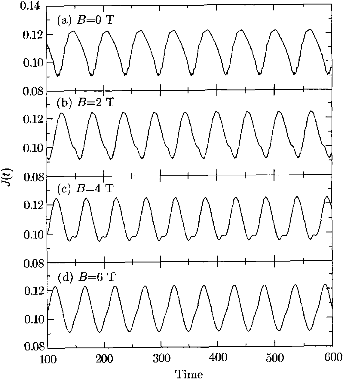
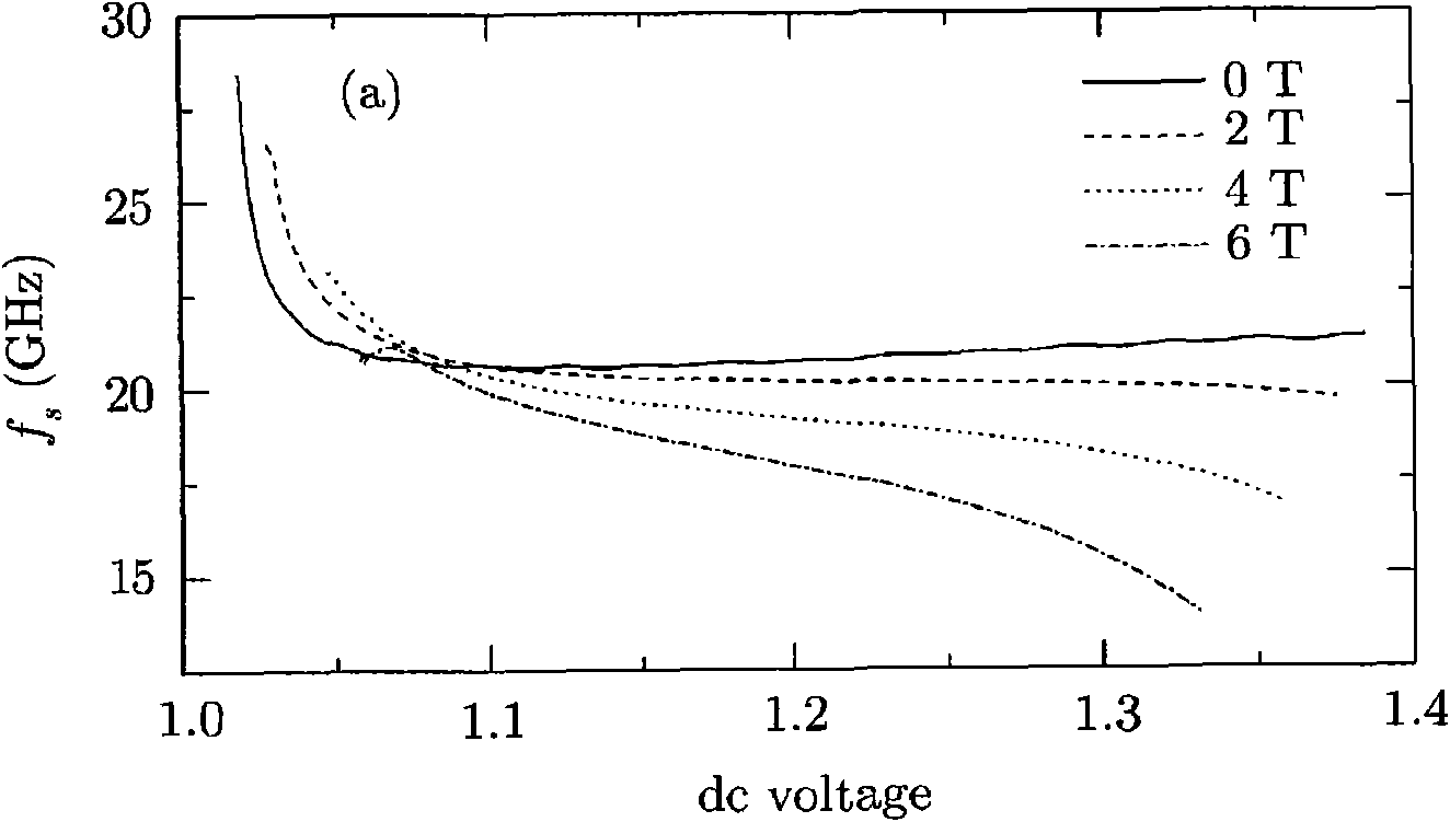
[0016] 3. Measure the I-V characteristics of the device in the presence of a magnetic field. Use a hig...


PUM


Abstract

The invention relates to a realization method of a tunable superlattice oscillator. The realization method is characterized in that (1) a current oscillation mode and an oscillation frequency in a superlattice oscillator are regulated by utilizing an externally-added magnetic field and an electric field, wherein, the superlattice oscillator is a weak coupling superlattice based on a resonance tunneling mechanism of a current carrier; (2) the direction of the externally-added magnetic field is vertical to that of the superlattice, the electric field is direct current bias voltage, and the direct current bias is along the growth direction of the superlattice; (3) the direct current bias voltage is fixed on the superlattice oscillator to produce zero damping oscillation current, and then the resonance frequency of the superlattice oscillator is continuously regulated by regulating the externally-added magnetic strength. To sum up, the invention can realize continuous change of the oscillation frequency of the superlattice oscillator by utilizing the regulation of the externally-added magnetic field and the electric field.

Description

technical field [0001] The invention relates to a realization method of a tunable superlattice oscillator, more precisely, relates to a method for adjusting the oscillation frequency of the superlattice oscillator by using the control of the magnetic field and the electric field on the electric field domain. This method has potential application value in the development of tunable oscillators based on semiconductor superlattice. Background technique [0002] Semiconductor superlattice [L.Esaki and R.Tsu, IBM J.Res.Dev.14, 61 (1970)] is a periodic semiconductor structure formed by alternate growth of two lattice-matched semiconductor materials. In the growth direction of the superlattice, if the potential barrier is narrow, the coupling between the bound energy levels of each quantum well will be stronger to form a microstrip. Under the action of an electric field, when electrons accelerate to the boundary of the Brillouin zone in the microstrip, the electrons have a negativ...

Claims


Application Information

Patent Timeline
IPC IPC(8): H03B28/00H01L29/15
Inventor 王长曹俊诚
Owner SHANGHAI INST OF MICROSYSTEM & INFORMATION TECH CHINESE ACAD OF SCI
Why Eureka
Try Eureka