Method for using screen plate for packaging and molding light emitting diode (LED)

A technology of light-emitting diodes and stencils, which is applied in the direction of electrical components, circuits, semiconductor devices, etc., can solve the problems of reduced production efficiency, cumbersome process, and increased equipment cost, and achieve the effects of reducing equipment cost, simplifying the process, and improving production efficiency

Inactive Publication Date: 2009-11-25
GENIUS ELECTRONICS OPTICAL CO LTD
View PDF0 Cites 23 Cited by
  • Summary
  • Abstract
  • Description
  • Claims
  • Application Information

AI Technical Summary

Problems solved by technology

[0004] It is true that the LED products obtained by the above-mentioned screen printing process have high light output quality and reliability, but with the increasingly diverse LED packaging structures, the above-mentioned screen printing process is no longer sufficient. Specifically, if the LED packaging structure has multiple phosphors For the adhesive layer and the light-transmitting adhesive layer, people must successively use multiple screens with holes of different sizes to print each adhesive layer sequentially before the package can be completed. However, this will inevitably result in cumbersome processes, reduced production efficiency, and equipment costs. increase, not in line with economic benefits

Method used


Image

  • Method for using screen plate for packaging and molding light emitting diode (LED)
  • Method for using screen plate for packaging and molding light emitting diode (LED)
  • Method for using screen plate for packaging and molding light emitting diode (LED)

Examples


Embodiment Construction

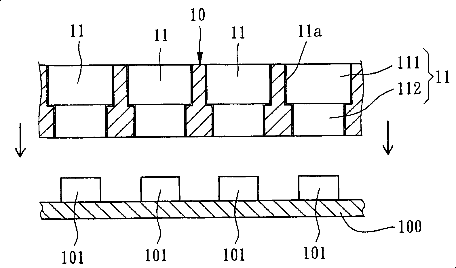
[0049] Please refer to Figure 1 to Figure 6 , is the first preferred embodiment of the present invention, which describes a method of using a mesh plate supplied in the packaging and molding process of light-emitting diodes, including the following steps:

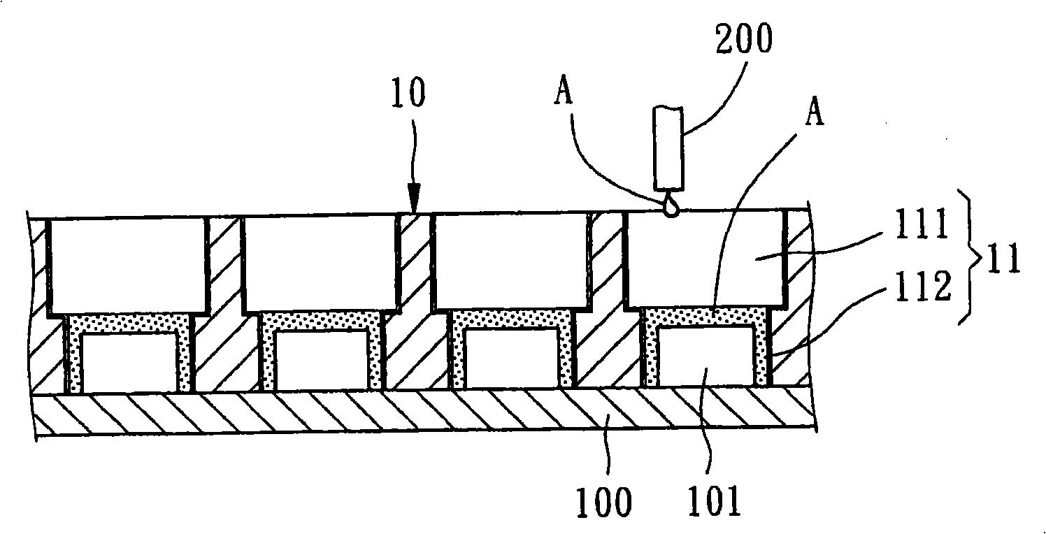
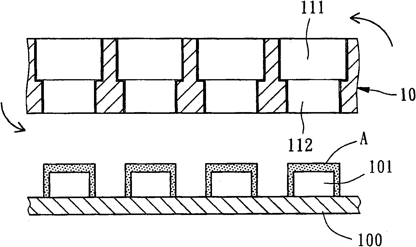
[0050] First, provide a net plate 10, such as figure 1 As shown, the mesh plate 10 has a plurality of step holes 11, each of which has a large aperture portion 111 and a small aperture portion 112, and the hole walls are pre-surface treated (in this embodiment, a layer of non-stick coating is coated). The material 11a) of the encapsulating adhesive material, in order to facilitate the release of the mold;

[0051] Next, with the reference figure 2 , continue to place the screen plate 10 on a substrate 100 carrying a plurality of light emitting diode chips 101, and make these light emitting diode chips 101 be located in the small aperture portion 112 of the corresponding step hole 11, and then use glue dispensing The ma...


PUM


Abstract

The invention relates to a method for using a screen plate for packaging and molding a light emitting diode (LED).The screen plate with a plurality of class holes is put on a substrate carrying a plurality of LED chips, wherein the class holes are provided with a large aperture part and a small aperture part, and the small aperture part and the large aperture part are sequentially utilized to respectively coat a first packaging glue material and a second packaging glue material onto the LED chips. The method can repeatedly use the same screen plate for coating a glue layer onto the LED chips so as to simplify the process, improve the production efficiency, reduce the equipment cost and meet the packaging requirement of diversified LED packaging structures.

Description

technical field [0001] The present invention is related to the process of light-emitting diodes, in detail, it refers to a method for using a screen used for encapsulating and molding light-emitting diodes. Background technique [0002] Press, LED (Light Emitting Diode) packaging operation includes the process of coating LED chips with fluorescent glue. Common processes include glue dispensing or mold casting. Among them, the package structure obtained by the glue dispensing process has problems of uneven size and colloidal displacement, resulting in poor light quality. Although the mold casting process does not have the above problems, However, the packaging process is prone to stress, resulting in poor contact between the LED chip and the substrate or even peeling off, resulting in poor reliability. Secondly, the equipment cost is also high. [0003] In order to improve the above defects, some operators have developed a process of coating fluorescent glue on the LED chip ...

Claims


Application Information

Patent Timeline
Patent Type & Authority Applications(China)
IPC IPC(8): H01L33/00H01L21/56
Inventor 陈明言魏梵修陈奉宽邱月霞吴晓雯
Owner GENIUS ELECTRONICS OPTICAL CO LTD
Why Eureka
Try Eureka