Display panel
A display panel and display area technology, applied in static indicators, nonlinear optics, optics, etc., can solve the problems of light leakage and small distance, and achieve the effect of avoiding light leakage
- Summary
- Abstract
- Description
- Claims
- Application Information
AI Technical Summary
Problems solved by technology
Method used
Image

Examples
no. 1 example
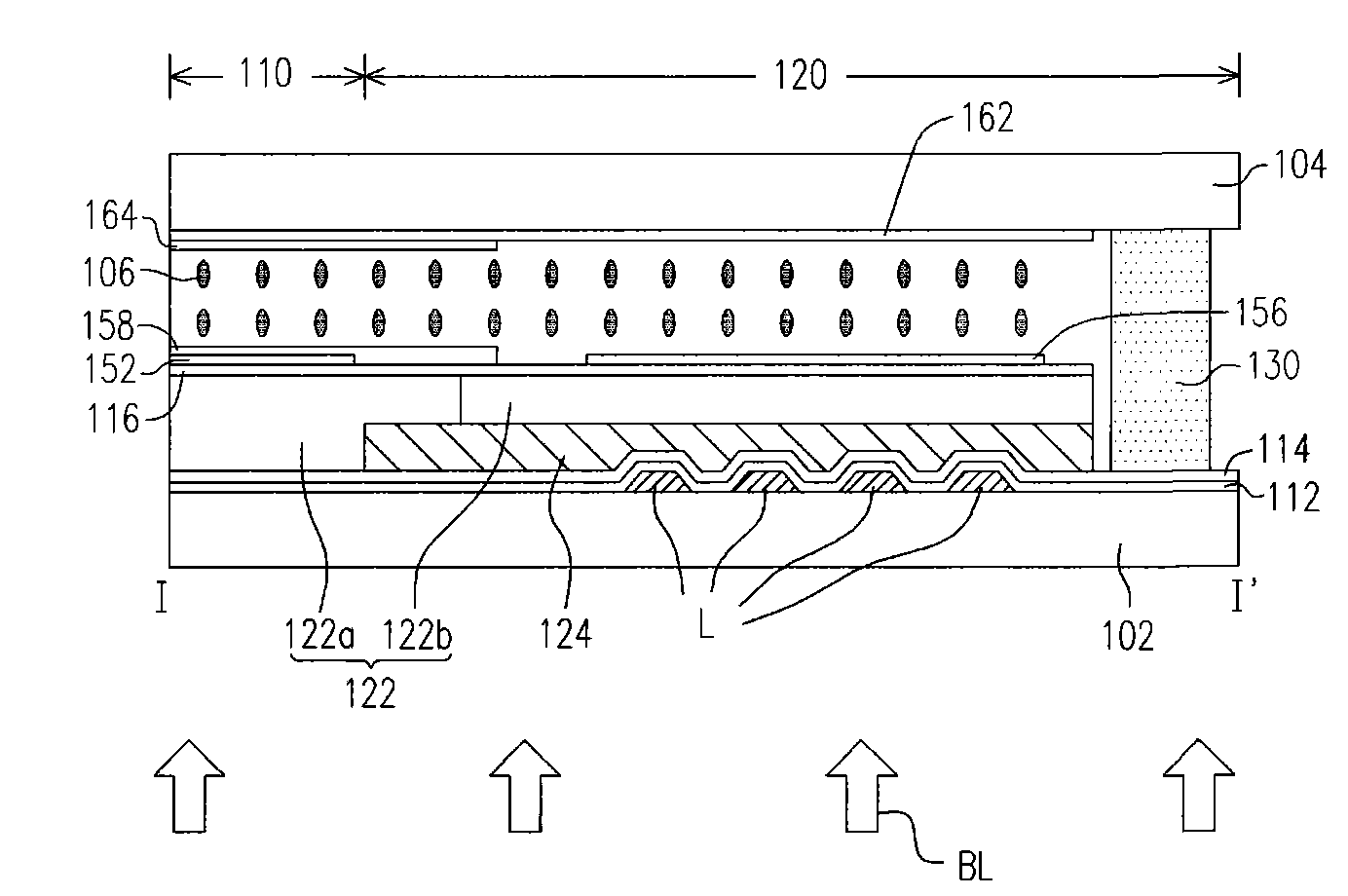
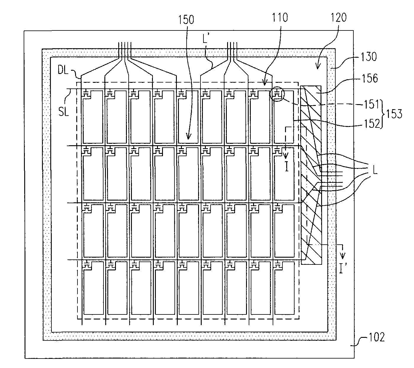
[0035] figure 1 is a partial cross-sectional schematic diagram of a display panel according to an embodiment of the present invention. figure 2 yes figure 1 A schematic top view of the first substrate of the display panel, wherein figure 1 for correspondence figure 2 at the section of I-I', and figure 2 The illustration of the color filter layer, the black matrix and the film layer thereon is omitted.
[0036] Please also refer to figure 1 as well as figure 2 , the display panel of this embodiment has a display area 110 and a non-display area 120 located around the display area 110 . That is to say, the non-display area 120 surrounds the display area 110 . The display panel includes a first substrate 102 , a second substrate 104 and a display medium 106 . In a preferred embodiment, the first substrate 102 and the second substrate 104 are assembled together through the sealant 130, and the display medium 106 is located between the first substrate 102 and the second ...
no. 2 example
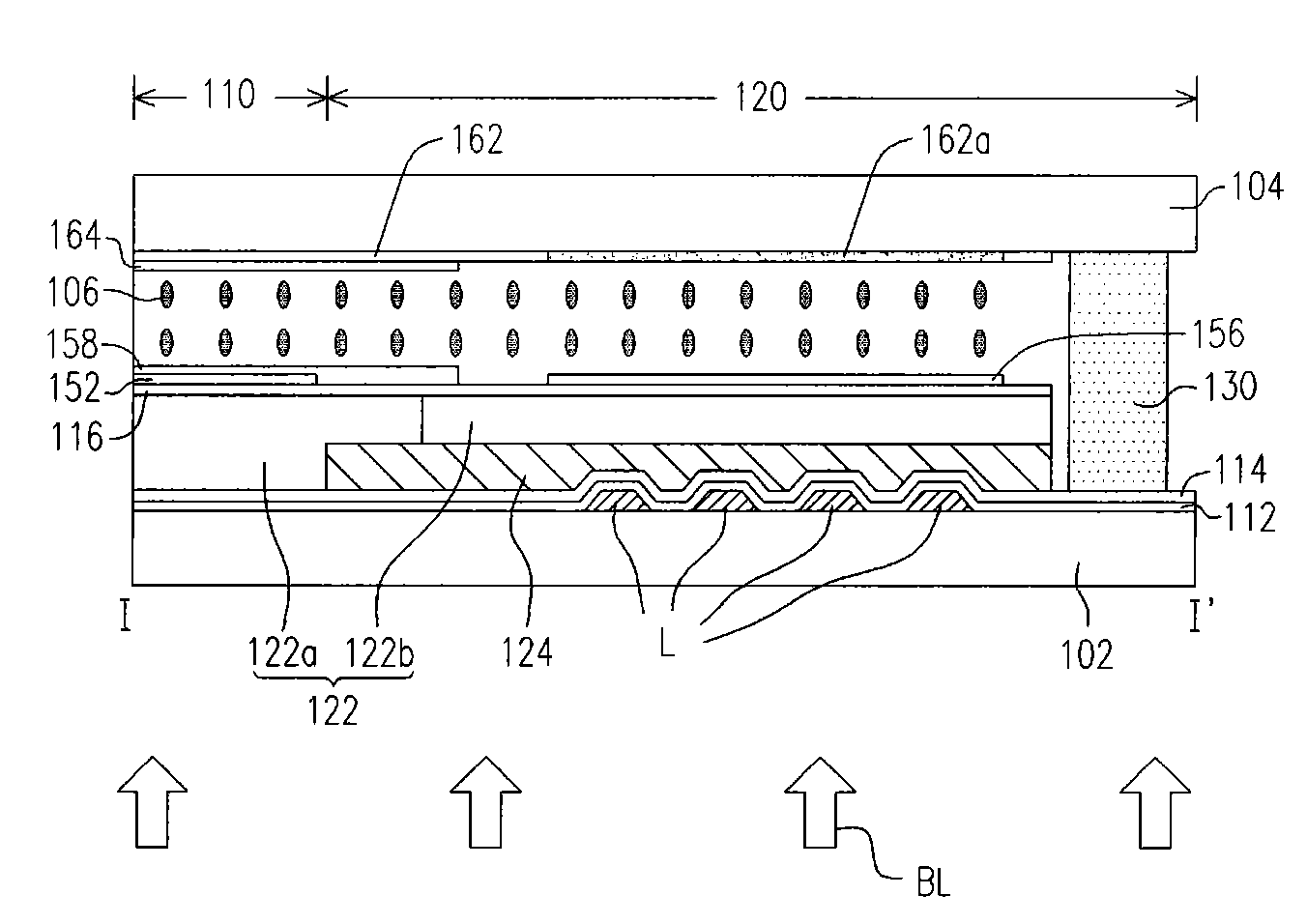
[0052] in the above figure 1 , image 3 as well as Figure 4 In the embodiment, the organic layer 122 is covered on the light-shielding pattern layer 124, but the present invention is not limited thereto. In other embodiments, the light-shielding pattern layer 124 may also cover the organic layer 122 . Please refer to Figure 5 , Figure 5 The embodiment of figure 1 Similar, the only difference is that the organic layer 122 is formed on the protective layer 114 , and the light-shielding pattern layer 124 is located on the organic layer 122 . In a preferred embodiment, the upper surface of the organic layer 122 is further covered with the protection layer 116 . In addition, in Figure 5 In an embodiment, the conductive pattern 156 is located between the light-shielding pattern layer 124 and the organic layer 122 (or the protection layer 116 ). Since the conductive pattern 156 can be formed together with the pixel electrode 152, the pixel electrode 152 is formed on the p...
no. 3 example
[0057] Figure 8 is a partial cross-sectional schematic diagram of a display panel according to an embodiment of the present invention. Figure 8 The embodiment of Figure 5Similar, except that the organic layer 122 above the lead L is not only designed with a conductive pattern 156, and the conductive pattern 156 and the electrode layer 164 are electrically connected to a common voltage, but also includes a pseudo-spacer 170 disposed on the conductive pattern 156. . In particular, there is a gap (A) between the pseudo-spacer 170 and the transparent electrode layer 162 on the second substrate 104 . If the display medium 106 in the display area 110 has a thickness (G), then the relationship between the gap (A) and the thickness (G) is A≧1 / 2G. The design of the pseudo-spacer 170 can displace the display medium (eg liquid crystal molecules) 106 above the lead L without affecting the thickness (G) of the display medium 106 in the display area 110 of the display panel. In addit...
PUM
 Abstract
Description
Claims
Application Information
 - R&D Engineer
- R&D Manager
- IP Professional
- Industry Leading Data Capabilities
- Powerful AI technology
- Patent DNA Extraction
Browse by: Latest US Patents, China's latest patents, Technical Efficacy Thesaurus, Application Domain, Technology Topic.
© 2024 PatSnap. All rights reserved.Legal|Privacy policy|Modern Slavery Act Transparency Statement|Sitemap