Active element matrix substrate
A technology of matrix substrates and active components, applied in nonlinear optics, instruments, optics, etc., can solve the problems affecting the brightness performance of liquid crystal display 100 and the decrease of pixel aperture ratio, so as to avoid light leakage, increase aperture ratio, and improve pixel aperture rate effect
- Summary
- Abstract
- Description
- Claims
- Application Information
AI Technical Summary
Problems solved by technology
Method used
Image
Examples
no. 1 example
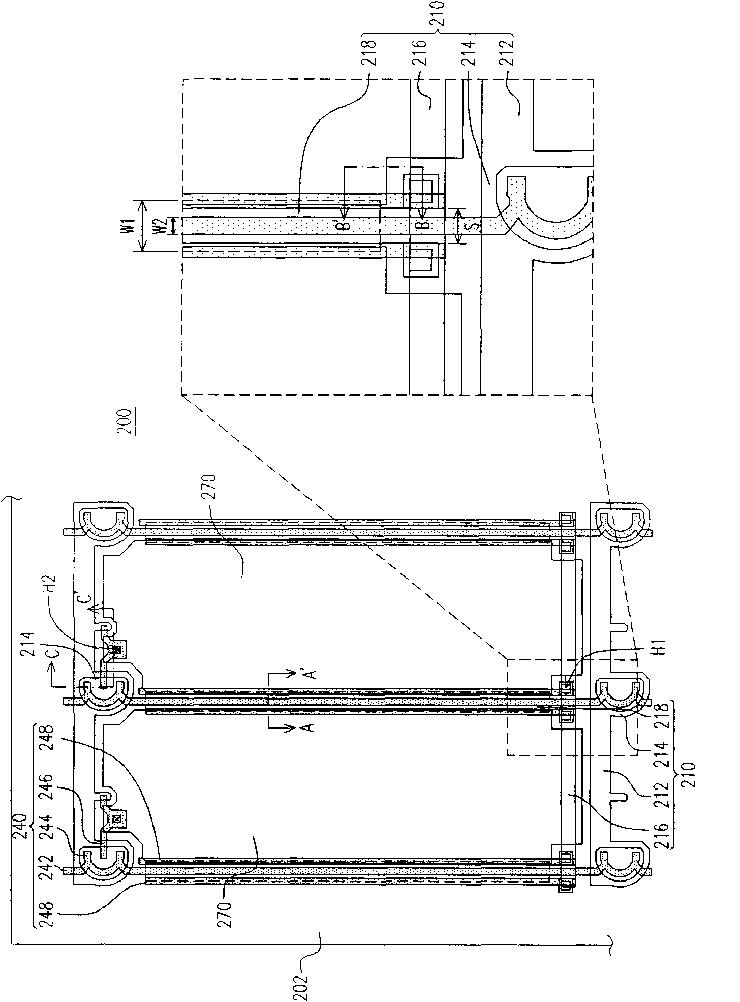
[0072] figure 2 It is a partial top view of an active element matrix substrate according to the first embodiment of the present invention, Figure 3A will be figure 2 The partial cross-sectional view of the active element matrix substrate applied to the liquid crystal display in Figure 3A The position of the mid-section is roughly along the figure 2 The corresponding position of the active element matrix substrate 200 of the cross-section line AA' in the middle. Please also refer to figure 2 and Figure 3A The active device matrix substrate 200 of this embodiment includes a substrate 202 , a first patterned conductor layer 210 , a dielectric layer 230 , a second patterned conductor layer 240 , a protection layer 260 and a plurality of pixel electrodes 270 .
[0073] Please also refer to figure 2 and Figure 3A , the first patterned conductor layer 210 is disposed on the substrate 202, the first patterned conductor layer 210 includes a plurality of scanning lines 2...
no. 2 example
[0086] Figure 4 It is a partial top view of an active element matrix substrate according to the second embodiment of the present invention, please refer to Figure 4 The active element matrix substrate 400 of this embodiment is similar to the active element matrix substrate 200 of the first embodiment. In the pixel unit of the active element matrix substrate 400 of this embodiment, the storage capacitor is in the form of a storage capacitor on the scanning line 212 type (Cst on scan line). For clarity, the same components in this embodiment and the first embodiment are denoted by the same symbols.
[0087] Figure 5 for Figure 4 Schematic cross-section along the BB' section line. Please refer to Figure 5 , in this embodiment, the position of the first contact opening H1 of the dielectric layer 230 is opened above the scan line 212 , in other words, the first contact opening H1 respectively exposes a part of the scan line 212 . Moreover, each strip capacitor electrode ...
PUM
 Abstract
Description
Claims
Application Information


