Multi-gap liquid crystal display panel and manufacturing method thereof

A technology of liquid crystal display panels and manufacturing methods, applied in semiconductor/solid-state device manufacturing, optics, instruments, etc., can solve problems such as complex processes, reduce brightness of liquid crystal displays, etc., and achieve the effect of solving dispersion

Active Publication Date: 2012-01-04
AU OPTRONICS CORP
View PDF2 Cites 0 Cited by
  • Summary
  • Abstract
  • Description
  • Claims
  • Application Information

AI Technical Summary

Problems solved by technology

However, either the process is too complicated, or it will reduce the brightness of the LCD

Method used


Image

  • Multi-gap liquid crystal display panel and manufacturing method thereof
  • Multi-gap liquid crystal display panel and manufacturing method thereof
  • Multi-gap liquid crystal display panel and manufacturing method thereof

Examples


Embodiment 1

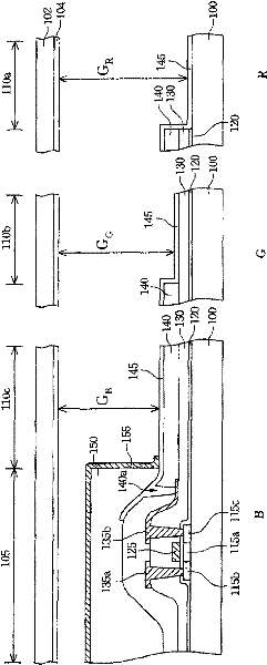
[0065] Please refer to Figure 1A , which shows a cross-sectional schematic diagram of a pixel structure of a transflective liquid crystal display according to an embodiment of the present invention. exist Figure 1A , the cross-sectional schematic diagram of red (R), green (G), and blue (B) three-color pixels is marked. Since the wavelengths of the three primary colors are red, green and blue in order from large to small, the height difference between the transmissive region 110a and the reflective region 105 of the red pixel (R) is the largest, at least the gate dielectric layer 120 , the sum of the thicknesses of the dielectric layer 130 , the passivation layer 140 and the organic planarization layer 150 . Secondly, the height difference between the transmissive region 110 b and the reflective region 105 of the green pixel (G) is at least the sum of the thicknesses of the protection layer 140 and the organic flat layer 150 . The minimum is the height difference between the...

Embodiment 2

[0074] Please refer to Figure 2A , which shows a cross-sectional schematic diagram of a pixel structure of a transflective liquid crystal display according to another embodiment of the present invention. exist Figure 2A , the cross-sectional schematic diagram of red (R), green (G), and blue (B) three-color pixels is marked. Similarly, since the wavelengths of the three primary colors of light are red, green, and blue in descending order, the height difference between the transmissive area 210a and the reflective area 205 of the red pixel (R) is the largest, at least for the gate interlayer. The total thickness of the electrical layer 220 , the passivation layer 245 and the organic planarization layer 260 . Secondly, the height difference between the transmissive area 210b and the reflective area 205 of the green pixel (G) and the blue pixel (B) is at least the thickness of the organic flat layer 260 .

[0075] Taking the red pixel as an example, the flow of a method for m...

Embodiment 3

[0080] In Embodiment 1 and Embodiment 2, the transparent electrode directly electrically connected to the drain metal is formed first, and then the reflective electrode directly electrically connected to the transparent electrode is formed. According to other embodiments, the reflective electrode directly electrically connected to the drain metal may also be formed first, and then the transparent electrode directly electrically connected to the reflective electrode may be formed. The present invention can also be applied to a transmissive liquid crystal display, forming a transparent electrode instead of the reflective electrode 265 .

[0081] Please refer to Figure 3A-3B , which shows a cross-sectional structural schematic diagram of a process flow of a manufacturing method of a pixel structure of a transflective liquid crystal display according to another embodiment of the present invention. because Figure 3A previous process and Figures 1A-1D Same, no more details her...


PUM

PropertyMeasurementUnit
thicknessaaaaaaaaaa
thicknessaaaaaaaaaa

Abstract

The invention provides a multi-gap liquid crystal display panel and a manufacturing method thereof. The manufacturing method comprises the following steps: providing a first substrate which is provided with a first pixel area, a second pixel area and a third pixel area; orderly forming a first dielectric layer and a second dielectric layer which are covered on the first pixel area, the second pixel area and the third pixel area; removing the second dielectric layer which is positioned on the second pixel area and the third pixel area; removing the first dielectric layer which is positioned onthe third pixel area; assembling a second substrate on the first substrate so as to form a first gap, a second gap and a third gap on the first pixel area, the second pixel area and the third pixel area between the first substrate and the second substrate respectively; and filling a liquid crystal layer between the first substrate and the second substrate. Different unit cell gaps are produced inthe pixel areas with different colors, so that the penetration rates of different color light tend to be consistent so as to solve the problem of chromatic dispersion.

Description

[0001] This application is a divisional application of an invention patent application with an application date of September 11, 2007, an application number of 200710148793.1, and an invention title of "multi-gap semi-transmissive reflective liquid crystal display and its manufacturing method". technical field [0002] The invention relates to a liquid crystal display and a manufacturing method thereof, in particular to a transflective liquid crystal display panel and a manufacturing method thereof. Background technique [0003] In order to solve the problem of display screen dispersion (chromatic dispersion) in the known transflective liquid crystal display, one of the solutions is to use one of the upper substrates of the liquid crystal display to manufacture some protrusions with different thicknesses to form a liquid crystal display with multiple cell gaps. To deal with the dispersion problem caused by the different wavelengths of the three primary colors. Another soluti...

Claims


Application Information

Patent Timeline
Patent Type & Authority Patents(China)
IPC IPC(8): G02F1/1333G02F1/1339G02F1/1335G02F1/13363H01L21/82
Inventor 林永伦董修琦
Owner AU OPTRONICS CORP
Why Eureka
Try Eureka