Mobile device of photoetching machine wafer stage and photoetching machine adopting mobile device

A mobile device and lithography machine technology, applied in the direction of micro-lithography exposure equipment, photolithography process exposure device, etc., can solve the problems of the frame burden of the whole machine, achieve low power requirements, and the effect of simple and easy moving in and out process

Active Publication Date: 2009-12-23
SHANGHAI MICRO ELECTRONICS EQUIP (GRP) CO LTD
View PDF0 Cites 31 Cited by
  • Summary
  • Abstract
  • Description
  • Claims
  • Application Information

AI Technical Summary

Problems solved by technology

In addition to the support frame of the wafer stage, and the cables, sensors, pipes, etc. designed to cooperate with the normal work of the corresponding components, the weight of the entire wafer stage can reach about 4 tons. It is necessary to directly assemble the wafer stage with the frame of the lithography machine Cause the burden of the whole frame

Method used


Image

  • Mobile device of photoetching machine wafer stage and photoetching machine adopting mobile device
  • Mobile device of photoetching machine wafer stage and photoetching machine adopting mobile device
  • Mobile device of photoetching machine wafer stage and photoetching machine adopting mobile device

Examples


Embodiment Construction

[0019] In order to make the object, technical solution and advantages of the present invention clearer, the present invention will be further described in detail below in conjunction with the accompanying drawings.

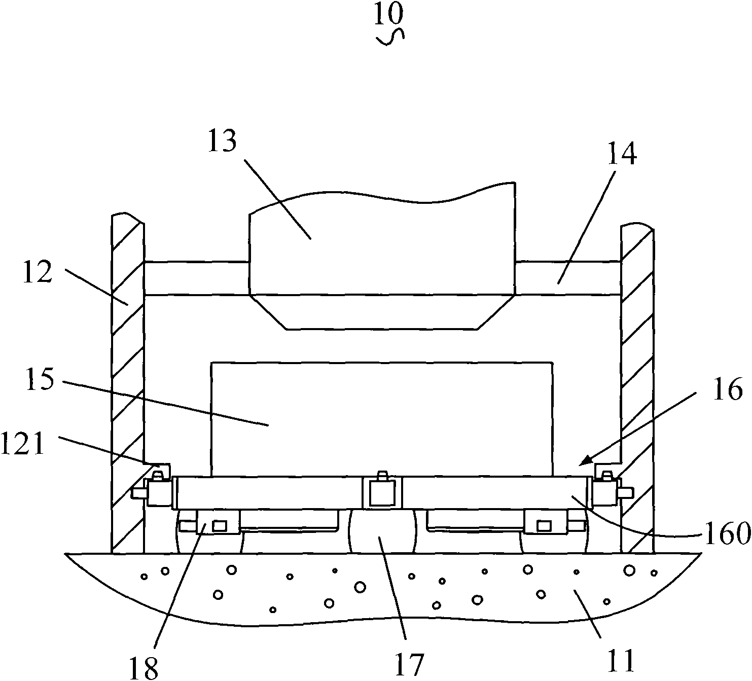
[0020] see figure 1 , figure 1 It is a structural schematic diagram of a photolithography machine using the silicon wafer stage moving device of the present invention. The lithography machine 10 includes a support frame 12 , an objective lens 13 , a main substrate 14 , a wafer stage 15 and a wafer stage moving device 16 . The support frame 12 is fixed on the foundation 11, the objective lens 13 and the main substrate 14 are arranged on the support frame 12, the wafer stage 15 is arranged below the objective lens 13, and the wafer stage moving device 16 carries the wafer stage 15 , for moving the wafer stage 15 into or out of the support frame 12 .

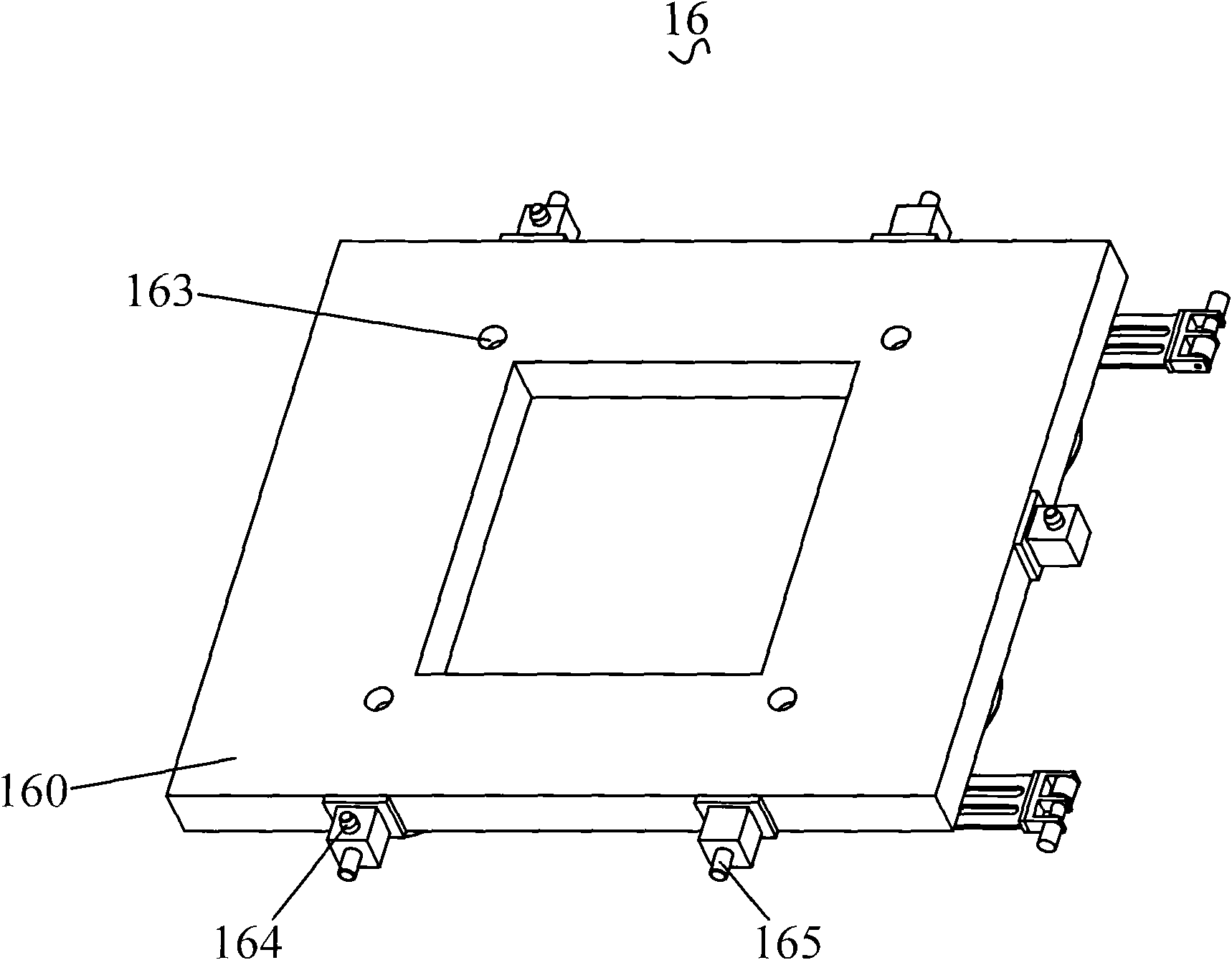
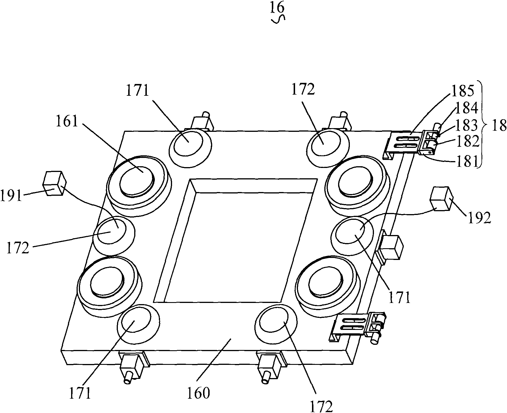
[0021] The wafer stage moving device 16 includes: a support plate 160 supporting the wafer stage 15; an airbag 17...


PUM


Abstract

The invention relates to a mobile device of a photoetching machine wafer stage and a photoetching machine adopting the mobile device. The mobile device of the photoetching machine wafer stage comprises a supporting plate supporting the photoetching machine wafer stage, an air pocket arranged on one side of the supporting plate opposite to the wafer stage, an air cushion device arranged on the side of the supporting plate same to the side of the air pocket, an idle wheel arranged on the side of the supporting plate same to the side of the air pocket; the air pocket is aerated and supports the supporting plate and the photoetching machine wafer stage; when the photoetching machine wafer stage is moved, the air pocket opens the air cushion device while releasing the gas; an air cushion formed by the air cushion device supports the supporting plate and the silicon stage; the mobile device of the photoetching machine wafer stage utilizes the idler wheel to shift out the wafer stage or shift the wafer stage into the photoetching machine. The shift-in and shift-out process of the wafer stage of the photoetching machine adopting wafer stage mobile device is simpler, can ensure the accurate locating of the wafer stage and a supporting frame of the photoetching machine and can reduce the disturbance of the ground vibration on the wafer stage.

Description

technical field [0001] The invention relates to a silicon wafer stage moving device of a lithography machine and a lithography machine using the moving device. Background technique [0002] Photolithography is a very important process in the semiconductor manufacturing process. It is a process of sequentially transferring chip patterns on a series of reticles to corresponding layers of silicon wafers through exposure. It is considered to be the core step in large-scale integrated circuit manufacturing. . A series of complex and time-consuming photolithography processes in semiconductor manufacturing are mainly completed by corresponding photolithography machines. The development of lithography technology or the technological progress of lithography machines mainly revolves around the three major indicators of line width, overlay accuracy and productivity. [0003] In the stepper projection lithography machine, the main purpose of the silicon wafer stage is to provide a mot...

Claims


Application Information

Patent Timeline
Patent Type & Authority Applications(China)
IPC IPC(8): G03F7/20
Inventor 秦磊刘育王天明袁志扬
Owner SHANGHAI MICRO ELECTRONICS EQUIP (GRP) CO LTD
Why Eureka
Try Eureka