

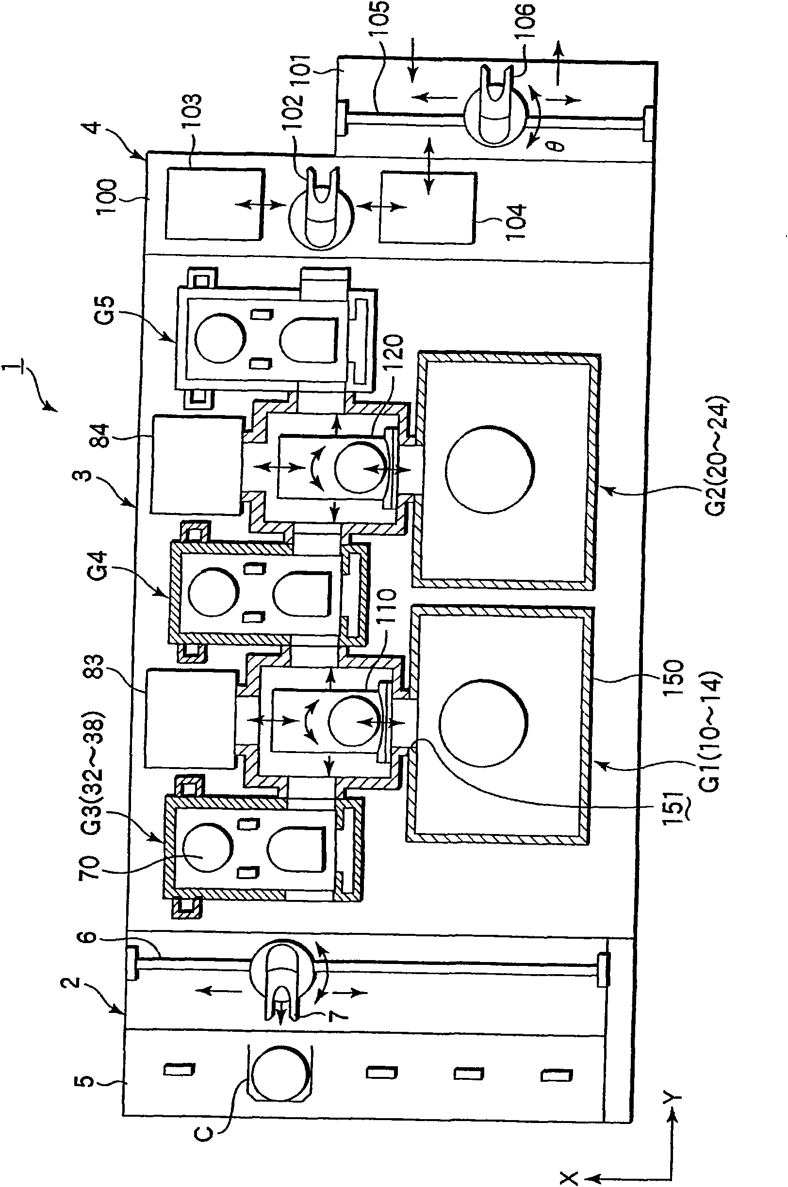
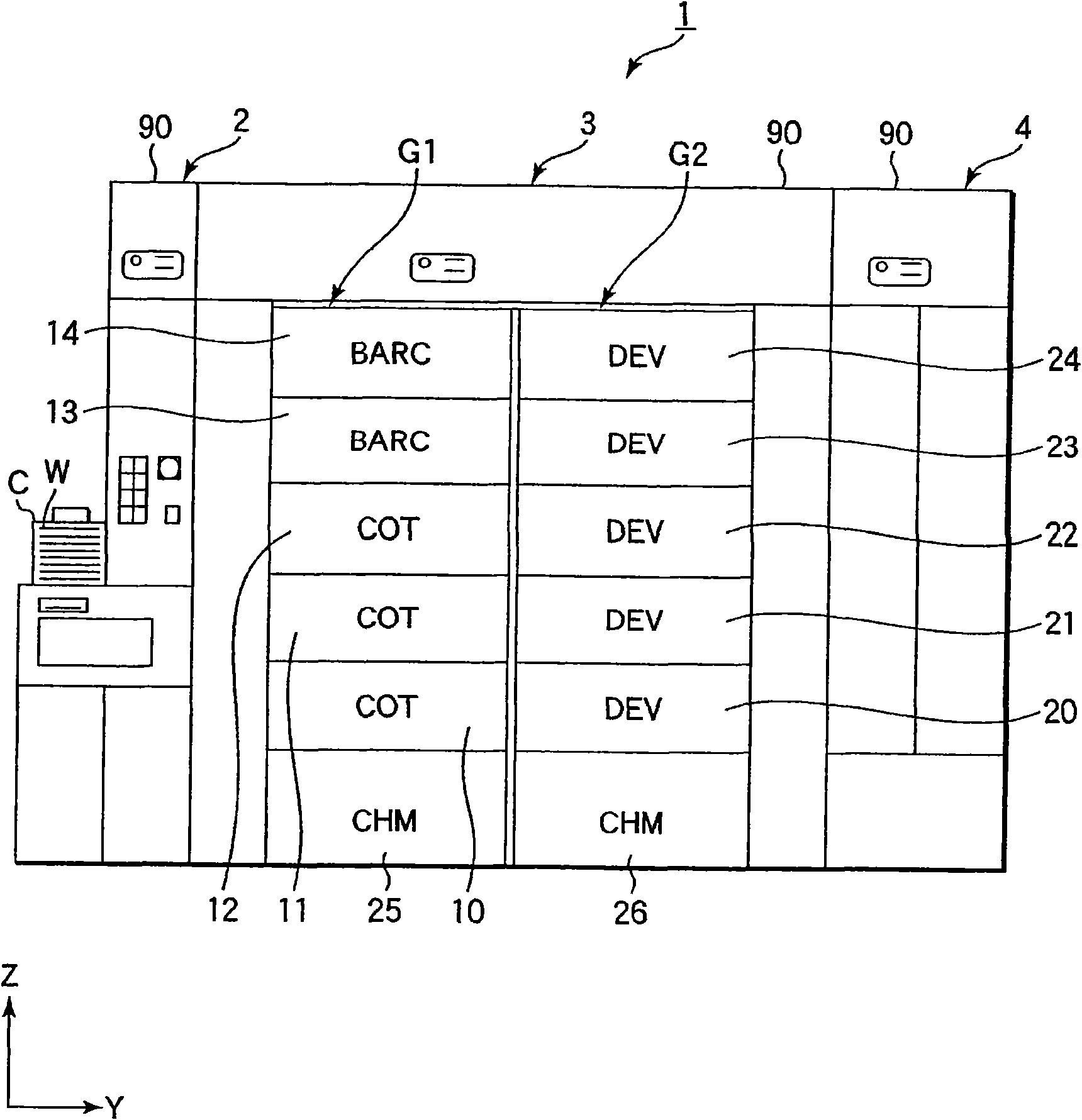
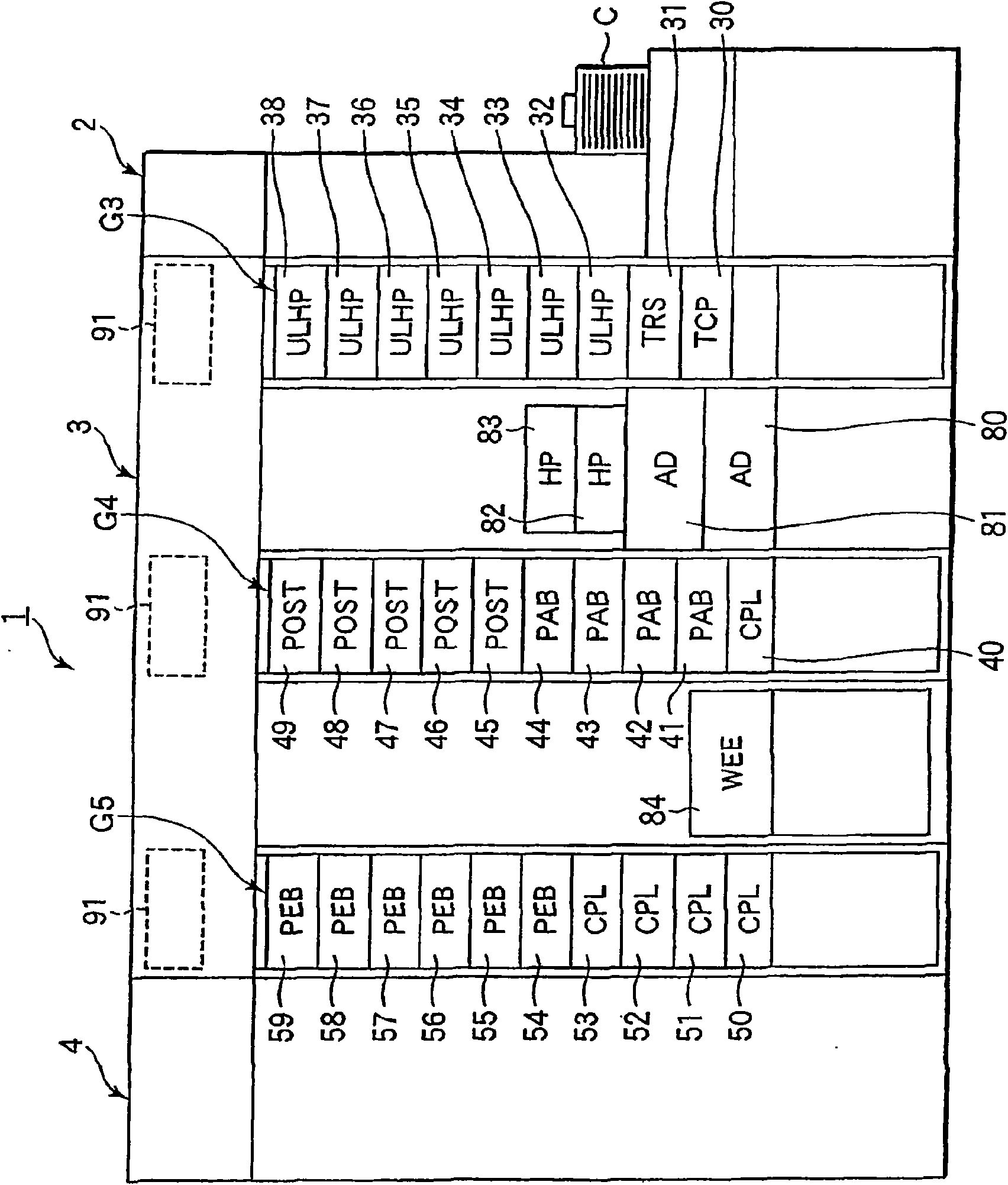
Substrate processing apparatus
A substrate processing device and substrate technology, applied in optics, instruments, optomechanical equipment, etc., can solve the problems of increased exhaust volume, inability to reduce exhaust volume, increase the number of coater covers, etc., to improve exhaust efficiency, The effect of preventing liquid mist
- Summary
- Abstract
- Description
- Claims
- Application Information
AI Technical Summary
Problems solved by technology
Method used
Image

Examples
no. 1 approach
[0061] Figure 4 is a schematic cross-sectional view showing a state during resist coating in the first embodiment of the resist coating processing apparatus 15, Figure 5 It is a schematic cross-sectional view showing a state of forming a resist film after supplying a resist.
[0062] The resist coating processing apparatus 15 includes: a spin chuck 16 that holds the wafer W horizontally by vacuum suction on its upper surface as a holding unit for the wafer W; A rotation mechanism 16b composed of, for example, a servo motor rotating in a horizontal plane; a processing liquid supply nozzle 17 (hereinafter referred to as coating nozzle 17) for supplying a resist to the surface of the wafer W; and a cleaning liquid such as pure water supplied to the surface of the wafer W. a cleaning nozzle (not shown); a backside cleaning nozzle (not shown) for supplying a cleaning solution such as pure water to the backside of the wafer W; an edge backside cleaning nozzle (not shown) for supp...
no. 2 approach
[0077] Figure 9 is a schematic cross-sectional view showing a state when the resist coating processing apparatus 15 is coating a resist in the second embodiment, Figure 10 It is a schematic cross-sectional view showing a resist film formation state after supplying a resist solution.
[0078] The second embodiment is formed using a plurality of vertically arranged rod-shaped members 76 capable of opening and closing the upper end openings of the respective air holes 66 , and an annular disc-shaped connecting member 77 connecting the upper ends of the respective rod-shaped members 76 to each other. The case of the opening and closing member 67A.
[0079] In this case, the rod member 76 passes through the through hole 62e provided on the inward flange portion 62d at the upper end of the cover 62, and its lower end closed portion has a narrow conical surface 76a that can be inserted into the vent hole 66. In this way, by providing the narrow conical surface 76a on the lower en...
no. 3 approach
[0087] Figure 13 is a schematic cross-sectional view showing a state when the resist coating processing apparatus 15 is coating a resist in the second embodiment, Figure 14 It is a schematic cross-sectional view showing a resist film formation state after supplying a resist solution.
[0088] The third embodiment is a case in which an opening and closing member is constituted by a member that opens and closes an annular air inlet 78 communicating with the vent hole 66 , for example, an annular member 79 .
[0089] In this case, the outer cover 62 includes an outer cover body 62d in which a vent hole 66 provided in the intermediate cover 64 communicates with the outer side of the outer cover 62 and an annular air inlet 78 is provided between the outer wall portion 62a. The annular member 79 that opens and closes the annular air inlet 78 formed by the exterior cover 62d and the outer wall portion 62a is provided with an elevating mechanism such as an elevating cylinder 68B ha...
PUM
 Abstract
Description
Claims
Application Information