Photoetching method capable of reducing width of exposure pattern

A technology for exposing graphics and width, which is applied in the direction of photosensitive materials, electrical components, semiconductor/solid-state device manufacturing for optomechanical equipment, etc., to achieve the effect of small width

Inactive Publication Date: 2010-02-03
SEMICON MFG INT (SHANGHAI) CORP
View PDF0 Cites 4 Cited by
  • Summary
  • Abstract
  • Description
  • Claims
  • Application Information

AI Technical Summary

Problems solved by technology

For example, when using a KrF laser light source with a wavelength of 193nm as the l

Method used


Image

  • Photoetching method capable of reducing width of exposure pattern
  • Photoetching method capable of reducing width of exposure pattern
  • Photoetching method capable of reducing width of exposure pattern

Examples


Embodiment Construction

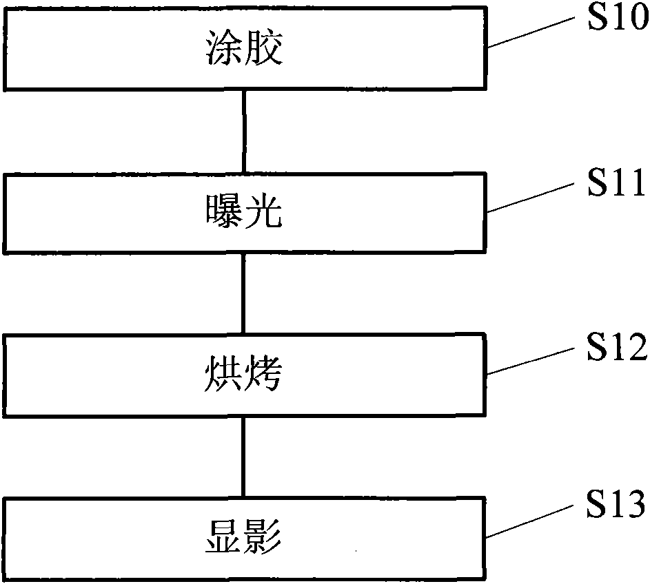
[0029] The specific implementation of the photolithography method for reducing the width of the exposure pattern provided by the present invention will be described in detail below in conjunction with the accompanying drawings.

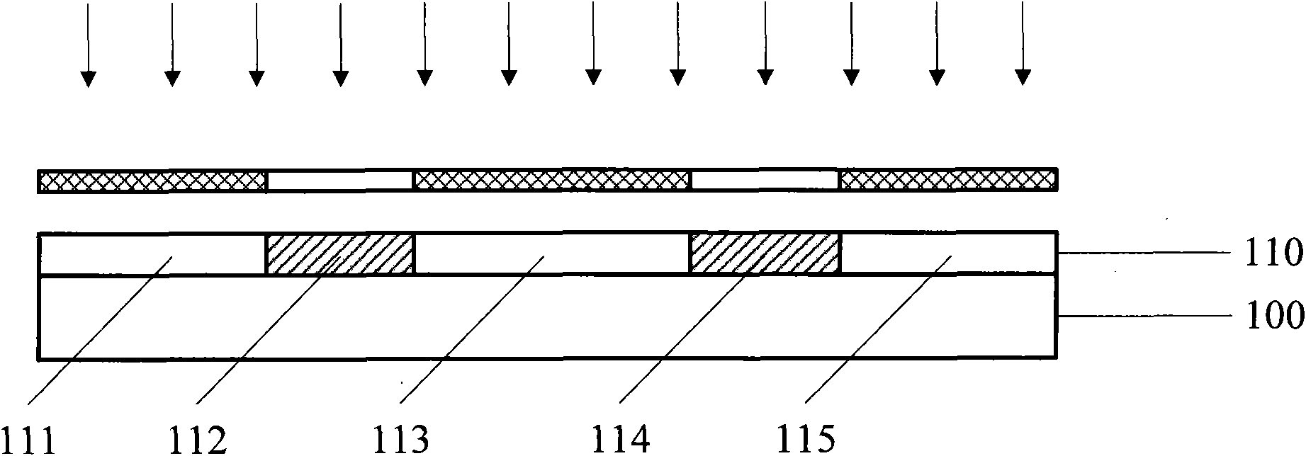
[0030] attached Figure 5 It is a process flow chart of a specific embodiment of the photolithography method for reducing the width of the exposure pattern in the present invention. Step S20, providing a semiconductor substrate with a photoresist layer on the surface; Step S21, exposing the photoresist layer to define patterns in the photoresist layer; Step S22, using a passivator containing trivalent nitrogen atoms and The photoresist layer after exposure undergoes a passivation reaction, and the trivalent nitrogen atoms in the passivation agent combine with hydrogen ions existing on the surface and sides of the exposed part of the photoresist layer to form The cladding layer; Step S23 , developing the passivated photoresist layer to remove the unex...


PUM

PropertyMeasurementUnit
Thicknessaaaaaaaaaa

Abstract

The invention provides a photoetching method capable of reducing the width of an exposure pattern. The method comprises the following steps of: providing a semiconductor substrate of which the surfaceis provided with a photoresist layer; exposing the photoresist layer, and defining a pattern in the photoresist layer; carrying out a passivation reaction of a passivating agent containing trivalentnitrogen atoms and the exposed photoresist layer to form a coating layer on the exposed surface and side surfaces of the photoresist layer for the trivalent nitrogen atoms in the passivating agent cancombine with the hydrogen ions on the exposed surface of the photoresist layer; and developing the passivated photoresist layer to remove the unexposed part of the photoresist layer and keep the coating layer and the exposed part of the photoresist layer coated by the coating layer. The method has the advantages that: because the passivating agent containing trivalent nitrogen atoms is used to becombined with the hydrogen ions on the exposed surface and side surfaces of the photoresist layer to form the coating layer, the pattern width of the unexposed part is reduced, the limitation of thewavelength on the minimum width is broken through, and the pattern with smaller width can be obtained.

Description

【Technical field】 [0001] The invention relates to the field of integrated circuit manufacturing, in particular to a photolithographic method for reducing the width of an exposure pattern. 【Background technique】 [0002] In the field of integrated circuit manufacturing, with the continuous reduction of the feature size of integrated circuits and the continuous improvement of chip integration, the traditional production mode, process materials and device models are facing many challenges. [0003] Photolithography is one of the most critical processes in the field of integrated circuit manufacturing. figure 1 Shown is a flow chart of the implementation steps of the photolithography process in the prior art, which generally includes the following steps: [0004] Step S10, applying glue; Step S11, exposing; Step S12, baking; Step S13, developing. [0005] attached figure 2 to attach Figure 4 Shown is a process schematic diagram of a photolithography process in the prior ar...

Claims


Application Information

Patent Timeline
IPC IPC(8): H01L21/027G03F7/09
Inventor 冯士祯崔彰日
Owner SEMICON MFG INT (SHANGHAI) CORP
Why Eureka
Try Eureka