Display device

A technology for display devices and thin film transistors, applied in optics, instruments, electrical components, etc., and can solve problems such as existence of boundaries

Active Publication Date: 2010-02-10
HITACHI DISPLAYS +1
View PDF1 Cites 7 Cited by
  • Summary
  • Abstract
  • Description
  • Claims
  • Application Information

AI Technical Summary

Problems solved by technology

[0010] Therefore, in the thin film transistor TFT constituted by the above structure, there is a limit in reducing its size

Method used


Image

  • Display device
  • Display device
  • Display device

Examples


Embodiment 1

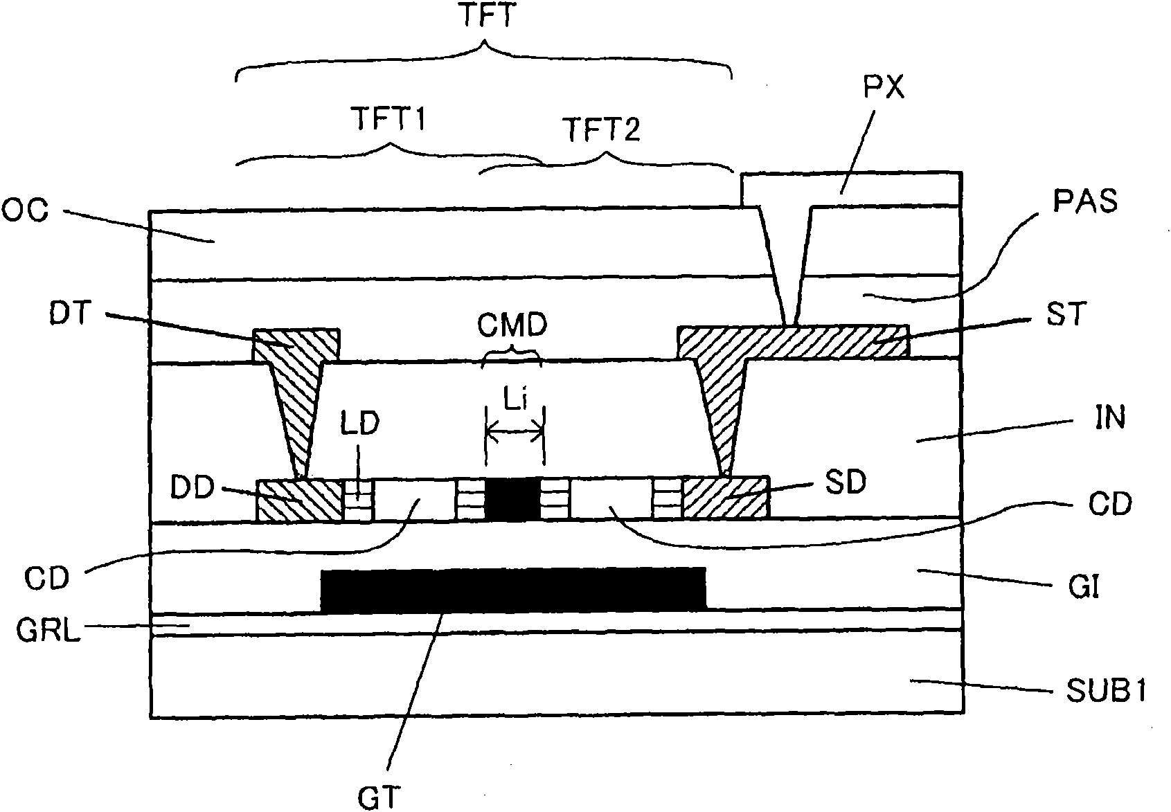
[0040] (The overall structure of the display device)

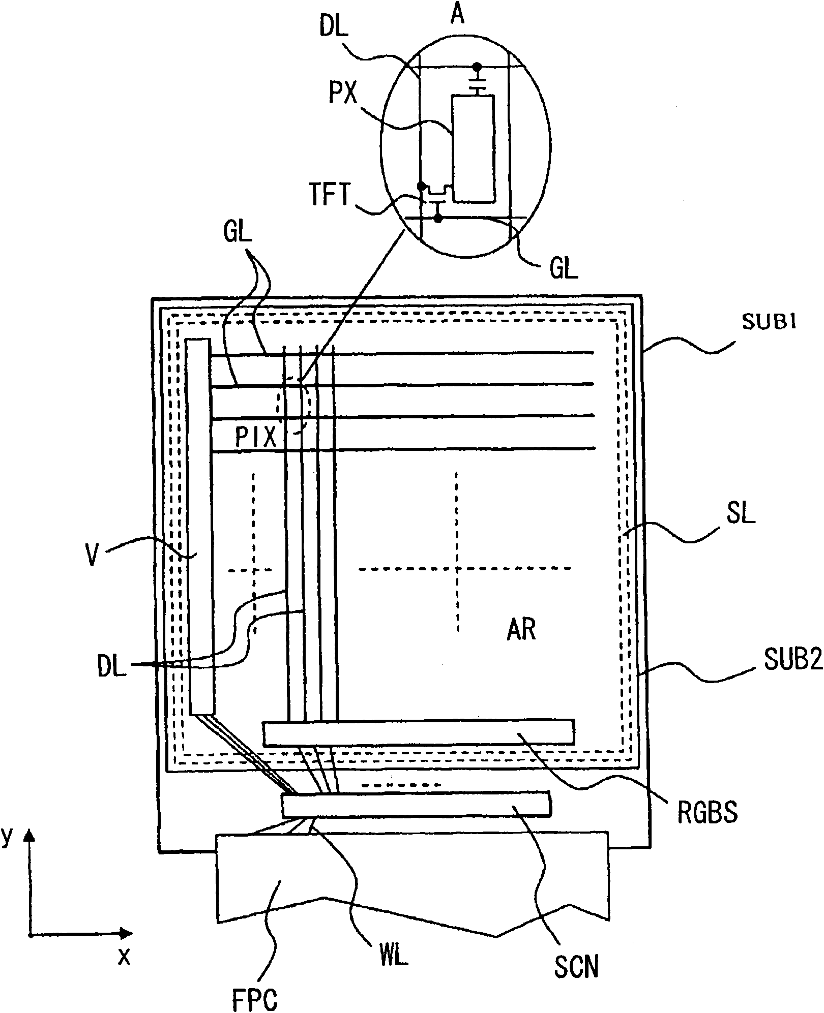
[0041] figure 2 It is a plan view of Example 1 of the display device of the present invention. figure 2 It is the overall structure of a liquid crystal display device embedded in a mobile phone, for example.

[0042] exist figure 2 Among them, the liquid crystal display device constitutes a case (peripheral) by rectangular-shaped substrates SUB1 and SUB2 made of, for example, glass. Liquid crystal (not shown) is sandwiched between the substrate SUB1 and the substrate SUB2, and the liquid crystal is enclosed by the sealing material SL that fixes the substrate SUB1 and the substrate SUB2. The region in which the liquid crystal is sealed by the sealing material SL constitutes the liquid crystal display region AR in the center except for a little periphery thereof. The liquid crystal display region AR is a region in which a plurality of pixels are arranged in a matrix.

[0043] The lower side of the substrate SUB1 has ...

Embodiment 2

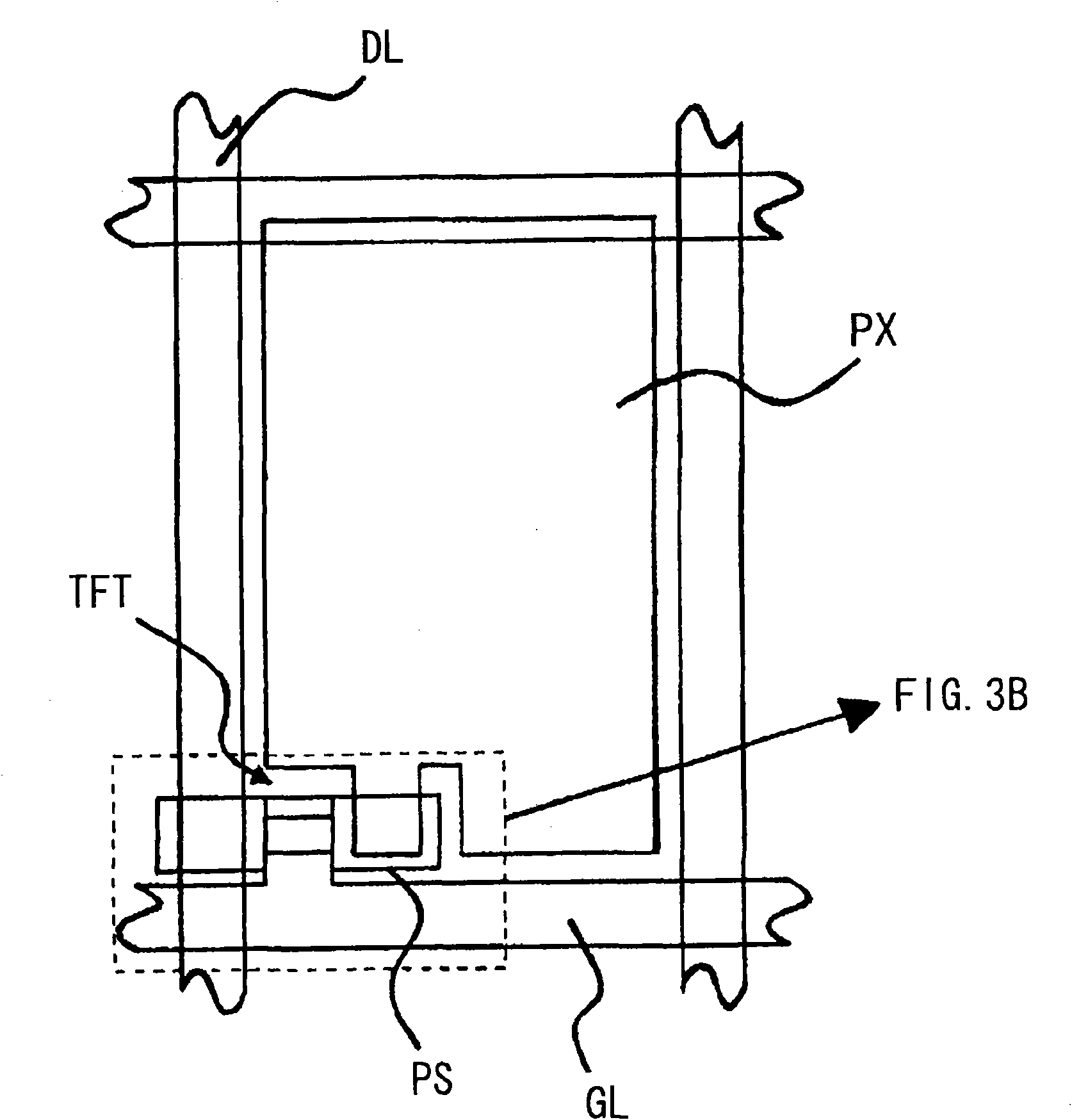
[0097] FIG. 7 is a structural diagram of Embodiment 2 of the display device of the present invention. Figure 7(a) is compared with figure 1 Correspondingly drawn, FIG. 7( b ) is a top view of the semiconductor layer PS of the thin film transistor TFT.

[0098] In Figure 7, with figure 1 Compared with the structure of TFT2, its different structure is that in the semiconductor layer PS, the drain region DD and the source region SD of the first thin film transistor TFT1, the drain region DD and the source region SD of the second thin film transistor TFT2 are respectively in the semiconductor layer PS formed as islands. The LDD region LD of the first thin film transistor TFT1 is formed to surround each of the drain region DD and the source region SD, and the LDD region LD of the second thin film transistor TFT2 is formed to surround each of the drain region DD and the source region SD.

[0099] Even in the case of such a structure, the gate electrodes GL of the first thin film ...


PUM


Abstract

An object of the present invention is to provide a display device where small thin film transistors with a lower off current can be formed. The present invention provides a display device where thin film transistors are formed on a substrate, and in the above described thin film transistors, a gate electrode is formed on a semiconductor layer with a gate insulating film in between, the above described thin film transistors are formed of at least a first thin film transistor and a second thin film transistor, and the above described semiconductor layer is divided into individual regions for each film transistor, the above described semiconductor layer is provided with a common region shared either by the drain region of the above described first thin film transistor and the source region of the above described second thin film transistor or by the source region of the above described first thin film transistor and the drain region of the above described second thin film transistor, in the first thin film transistor and the second thin film transistor, the semiconductor layer is provided with LDD regions where the impurity concentration is lower than in the above described drain region and the above described source region, between the channel region and the drain region, as well as between the channel region and the source region, and the above described gate electrode is formed so as to overlap with the above described common region in the above described semiconductor layer and face at least the above described channel region and the above described LDD regions of the above described first thin film transistor and the above described channel region and the above described LDD regions of the above described second thin film transistor.

Description

[0001] This application claims the benefit of Japanese Patent Application Japanese Patent Application No. 2008-202525 filed on August 6, 2008, the contents of which are hereby incorporated by reference. technical field [0002] The present invention relates to a display device, in particular to a display device with a thin film transistor formed in a substrate. Background technique [0003] For example, in an active matrix liquid crystal display device, a thin film transistor including a switching element is formed in the region of each pixel on the substrate. [0004] In this case, the thin-film transistor is preferably a so-called bottom-gate transistor in which a gate electrode is disposed on the substrate side with a gate insulating film interposed therebetween relative to the semiconductor layer. This is because the gate electrode functions as a light-shielding film, which prevents light from the backlight from being irradiated to the semiconductor layer, and constitute...

Claims


Application Information

Patent Timeline
Patent Type & Authority Applications(China)
IPC IPC(8): G02F1/1362G02F1/1368H01L27/12
CPCG02F2202/104G02F1/13624G02F1/136
Inventor 野田刚史宫泽敏夫海东拓生紫垣匠
Owner HITACHI DISPLAYS
Why Eureka
Try Eureka