Check patentability & draft patents in minutes with Patsnap Eureka AI!

Thin film transistor array substrate and LCD

A technology of thin-film transistors and array substrates, which is applied in the field of liquid crystal display devices and thin-film transistor array substrates, and can solve problems such as greatly affecting display quality and product performance, and reducing display brightness.

Active Publication Date: 2010-02-17
INNOLUX CORP
View PDF2 Cites 8 Cited by
  • Summary
  • Abstract
  • Description
  • Claims
  • Application Information

AI Technical Summary

Problems solved by technology

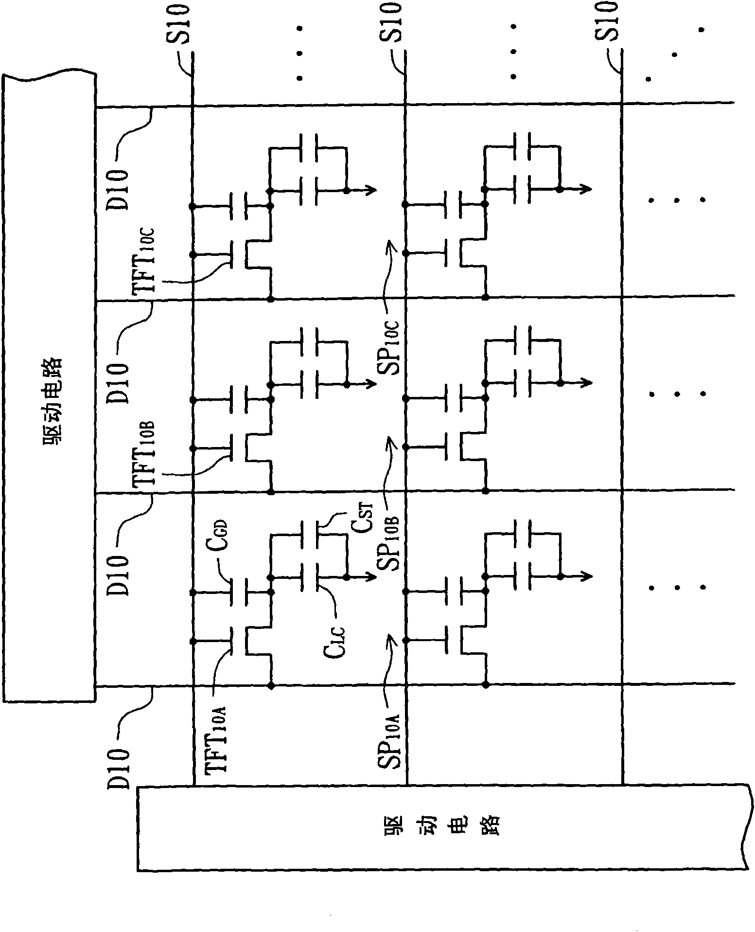
In this way, the sub-pixel SP 20A 、SP 20B with SP 20C Although you can get a C ST-A =C ST-B =C ST-C results in maintaining the feedthrough voltage V FD-A ≈V FD-B ≈V FD-C However, the aperture ratio of the remaining sub-pixels will be sacrificed and the overall display brightness will be reduced, which will greatly affect the display quality and product performance.

Method used


Image

  • Thin film transistor array substrate and LCD
  • Thin film transistor array substrate and LCD
  • Thin film transistor array substrate and LCD

Examples


no. 1 example

[0020] Please refer to image 3, which shows a side view of a liquid crystal display device according to the first embodiment of the present invention. The liquid crystal display device 100 of this embodiment includes a thin film transistor array substrate 40 , an opposite substrate 20 , spacers 10 and a liquid crystal layer 30 . The spacer 10 is arranged on the surface of the opposite substrate 20 facing the thin film transistor array substrate 40, and contacts the thin film transistor array substrate 40, so that there is a fixed distance between the thin film transistor array substrate 40 and the opposite substrate 20, and the liquid crystal layer 30 Filled and distributed between the opposite substrate 20 and the thin film transistor array substrate 40 , the spacers 10 are preferably photosensitive resin and formed by photolithography.

[0021] Figure 4 A top view of the thin film transistor array substrate 40 according to the first embodiment of the present invention is...

no. 2 example

[0036] The difference between this embodiment and the above-mentioned embodiments lies in the technical means adopted for uniform feed-through voltage, especially in the case of not changing the storage capacitive coupling area, only by changing the shape of the capacitor electrode to achieve uniform feed-through voltage and At the same time, the purpose of providing a space for the spacer is provided. Figure 6 A top view of a thin film transistor array substrate according to a second embodiment of the present invention is shown.

[0037] Please refer to Figure 6 The plurality of capacitor electrodes at least include a first capacitor electrode 44a, a second capacitor electrode 44b, and a third capacitor electrode 144c respectively located on the first conductive portion 42a, the second conductive portion 42b, and the third conductive portion 42c. The capacitor electrode 44a , 44b, 44c are coupled with conductive parts 42a, 42b, 42c to form a plurality of pixel storage capa...


PUM


Abstract

The invention provides a thin film transistor array substrate and an LCD. A plurality of scan lines and a plurality of data lines orthogonally define a first sub-pixel area, a second sub-pixel area and a third pixel area. A patterned conducting layer is formed on the substrate, and comprises a first conducting part, a second conducting part and a third conducting part which are respectively located in the first sub-pixel area, the second sub-pixel area and the third sub-pixel area; a plurality of capacitor electrodes comprise a first capacitor electrode, a second capacitor electrode and a third capacitor electrode which are respectively located above the first conducting part, the second conducting part and the third conducting part; the capacitor electrodes and the patterned conducting layer are coupled as a plurality of pixel storage capacitors; and a spacer is arranged above the third capacitor electrode, wherein, the shape of the third capacitor electrode is different from the shape of the first capacitor electrode and the shape of the second capacitor electrode, and the maximum width of the third capacitor electrode in the extension direction of the pattered conducting layer is larger than that of the first capacitor electrode and the second capacitor electrode in the extension direction of the pattered conducting layer.

Description

technical field [0001] The invention relates to a liquid crystal display device and a thin film transistor array substrate thereof, and in particular to a liquid crystal display device and a thin film transistor array substrate capable of preventing flickering. Background technique [0002] figure 1 A schematic circuit diagram of a general thin film transistor liquid crystal display device is shown. Please refer to figure 1 , the sub-pixels SP located on the same column of the general liquid crystal display device 10A 、SP 10B 、SP 10C Thin Film Transistor TFT of ... 10A 、TFT 10B 、TFT 10C ...are all driven by the same scan line (scan line) S10, usually a main pixel is composed of three sub-pixels, for example, a main pixel that can display any desired color is usually composed of three sub-pixels of red, green and blue composition. When the scan line S10 provides a sufficient turn-on voltage, the thin film transistor TFT connected to the scan line S10 10A 、TFT 10B 、...

Claims


Application Information

Patent Timeline
IPC IPC(8): G02F1/1362H01L27/12H01L21/84
Inventor 高毓谦
Owner INNOLUX CORP
Features
  • R&D
  • Intellectual Property
  • Life Sciences
  • Materials
  • Tech Scout
  • Unparalleled Data Quality
  • Higher Quality Content
  • 60% Fewer Hallucinations
Learn More