

Method for measuring focal plane uniformity of exposure machine
A focal plane and uniformity technology, which is applied in the field of measurement of the focal plane uniformity of exposure machines in semiconductor manufacturing, can solve the problems of less sampling, insufficient representation, and low measurement efficiency, so as to improve efficiency, sensitivity and accuracy , Overcome the single effect of graphics
- Summary
- Abstract
- Description
- Claims
- Application Information
AI Technical Summary
Problems solved by technology
Method used
Image

Examples
Embodiment Construction
[0029] The implementation of the present invention is described below through specific examples and in conjunction with the accompanying drawings, and those skilled in the art can easily understand other advantages and effects of the present invention from the content disclosed in this specification. The present invention can also be implemented or applied through other different specific examples, and various modifications and changes can be made to the details in this specification based on different viewpoints and applications without departing from the spirit of the present invention.
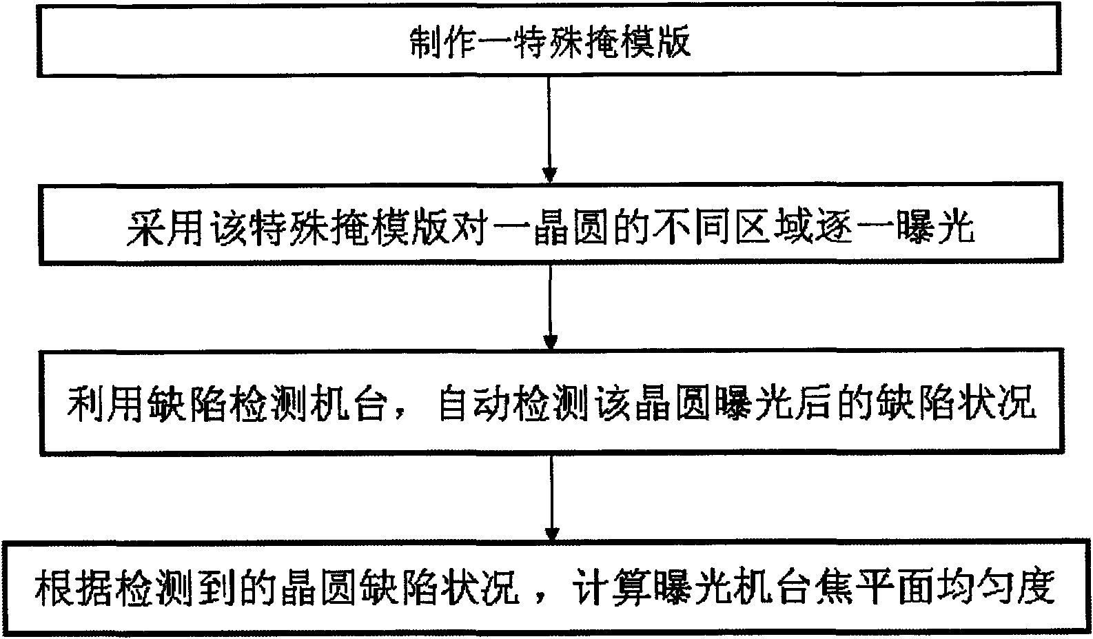
[0030] figure 2 It is a flow chart of a method for measuring the uniformity of the focal plane of an exposure machine in the present invention. The present invention is a method for measuring the uniformity of the focal plane of an exposure machine, comprising the following steps:
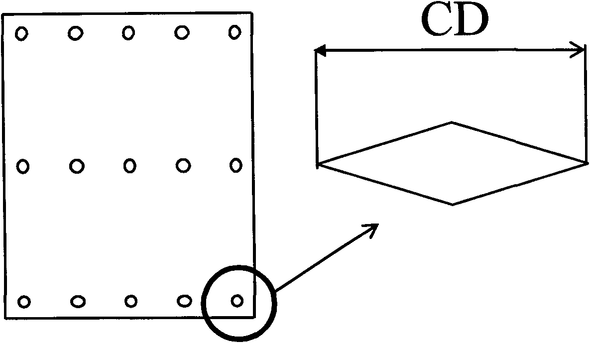
[0031] First, make a special mask. The pattern area of the mask is designed in combination with the lens ...
PUM
 Abstract
Description
Claims
Application Information