HBT structure with controllable working frequency in RF field

A technology of working frequency and field, applied in the field of the preparation of heterojunction bipolar transistors, can solve the problems of inability to adjust the working frequency, uncontrollable emitter-base change, and no controllability.

Active Publication Date: 2010-02-17
SHANGHAI HUAHONG GRACE SEMICON MFG CORP
View PDF0 Cites 1 Cited by
  • Summary
  • Abstract
  • Description
  • Claims
  • Application Information

AI Technical Summary

Problems solved by technology

[0003] The operating frequency of the above-mentioned existing HBT devices varies too slowly with the change of the emitter-collector voltage and does not have controllability ( image 3 shown), while the change with emitter-base is too fast to be controlled ( figure 2 shown), so the existing HBT devices usually can only work at a specific operating frequency, and cannot adjust the operating frequency by applying an external voltage

Method used


Image

  • HBT structure with controllable working frequency in RF field
  • HBT structure with controllable working frequency in RF field
  • HBT structure with controllable working frequency in RF field

Examples


Embodiment Construction

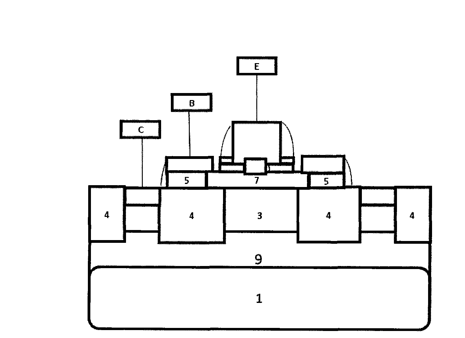
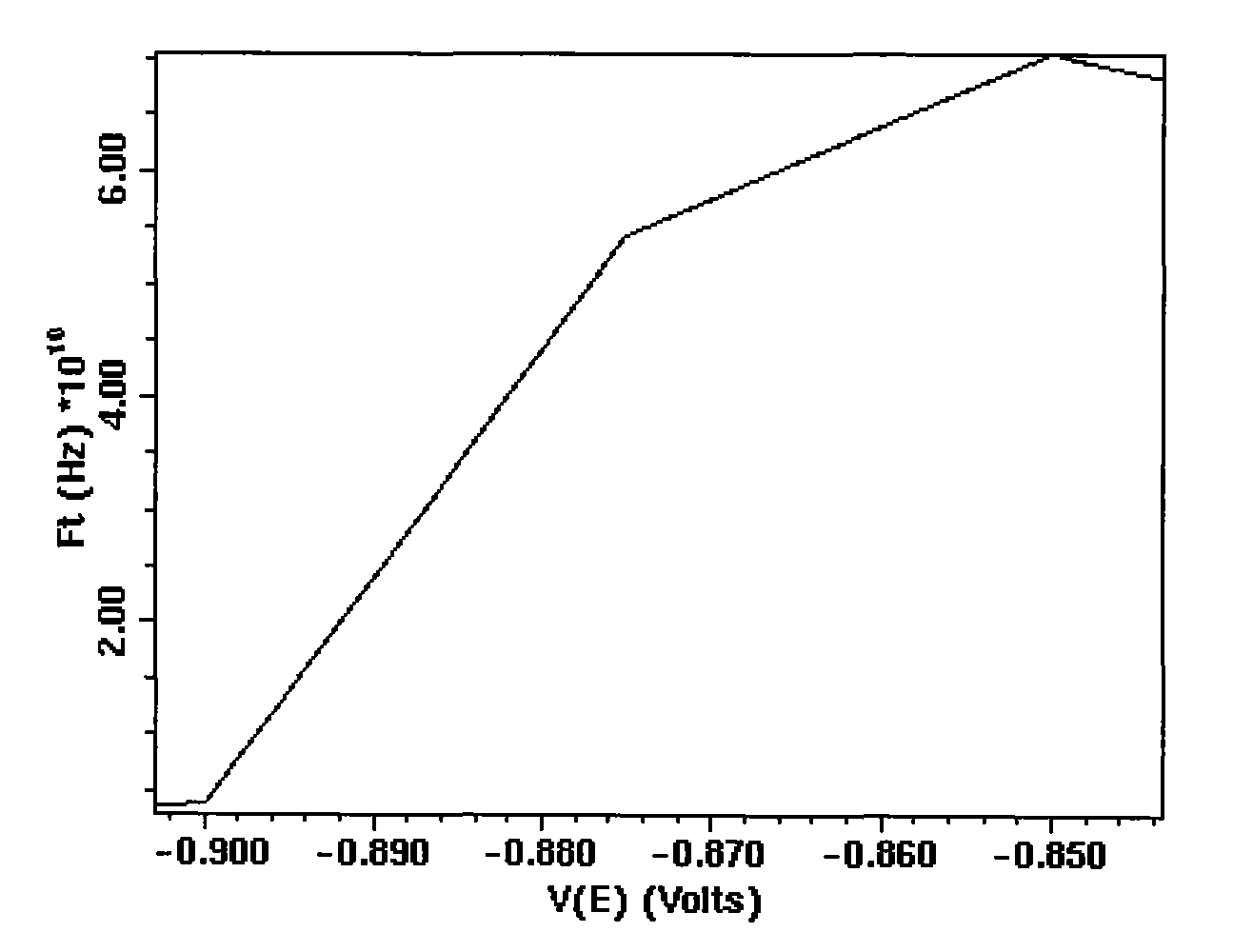
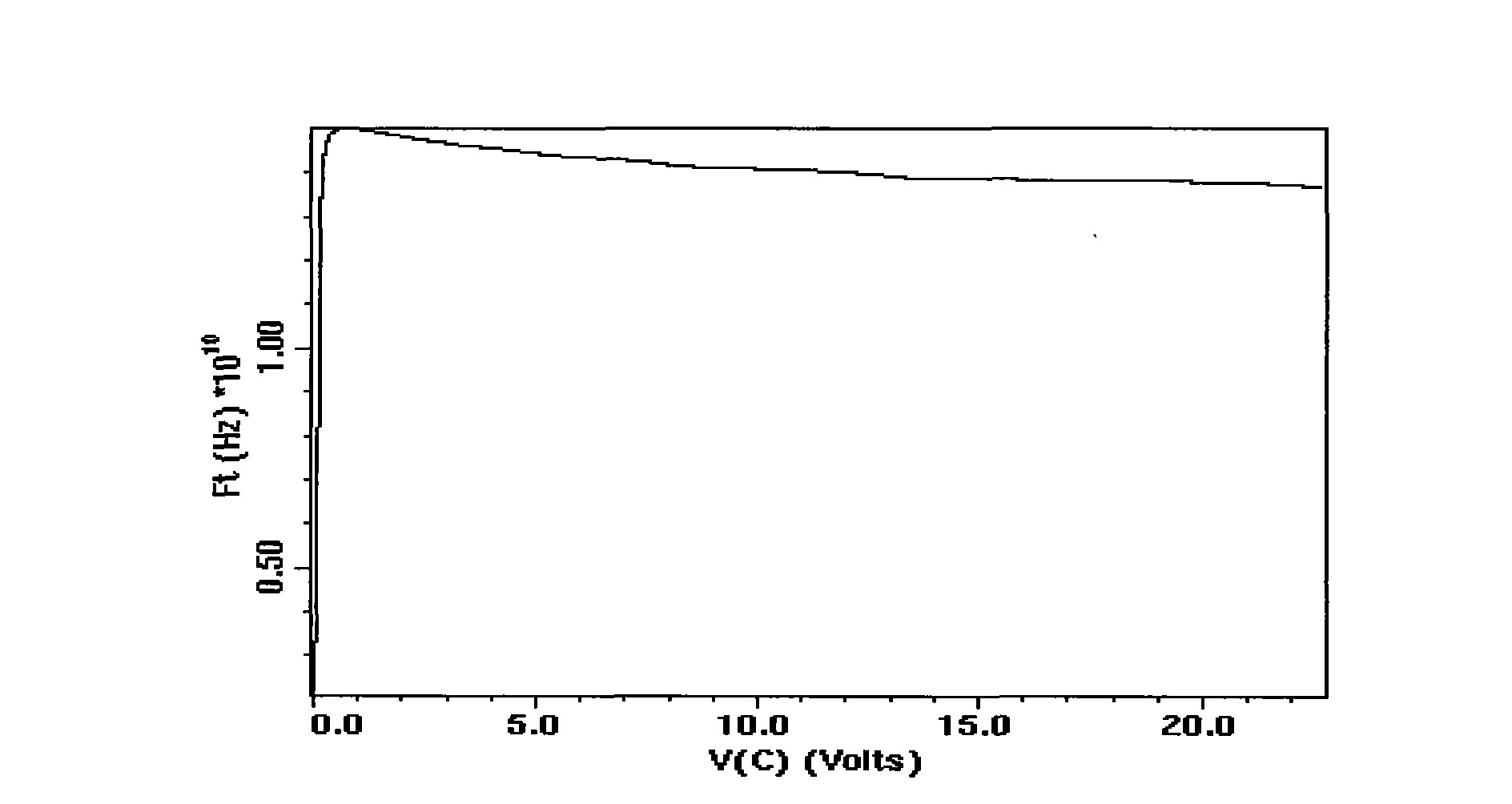
[0014] Such as Figure 4 As shown, the HBT structure with controllable operating frequency used in the RF field of the present invention is to implant high-concentration P-type impurities between the P-type substrate 1 and the collector region 3 of the existing HBT to form a high-concentration P-type The impurity buried layer 2 and the depletion line 8 are in the collector region 3.

[0015] Preferably, the high-concentration P-type impurity buried layer 2 has a thickness of not less than 1e19 cm -3 The impurity concentration.

[0016] Preferably, the distance 6 from the high-concentration P-type impurity buried layer to the shallow trench isolation is 600 nm to 1000 nm.

[0017] Preferably, the high-concentration P-type impurity buried layer 2 has a film thickness of 150 nm to 200 nm.

[0018] The HBT structure with controllable operating frequency used in the RF field of the present invention can be manufactured by a common process in the semiconductor field, and the manufacturing m...


PUM


Abstract

The invention discloses an HBT structure with controllable working frequency in the RF field, comprising a high-concentration P-type impurity buried layer injected between a P-type substrate and a collector region. By injecting high-concentration P-type impurity in an npn-type HBT device, the invention leads a longitudinal electrical filed in the device and realizes control of voltage on working frequency by the way that collector voltage controls the electrical field.

Description

Technical field [0001] The invention relates to a semiconductor device and an integrated circuit manufacturing process, in particular to a method for preparing a Heterojunction Bipolar Transistor (HBT) with a controllable operating frequency in the radio frequency (RF) field. Background technique [0002] Such as figure 1 Shown is the structure diagram of the existing HBT: a high-concentration N-type impurity buried layer 9 is implanted on the p-type substrate 1 as a collector region, and N-type impurity implantation forms an N-type collector 3, and shallow trench isolation The (STI)4 structure electrically isolates the unit HBT. A P-type SiGe epitaxial layer 7 is grown on the collector region 3, an oxide spacer 5 is formed around the p-type SiGe epitaxial layer 7, and an emitter region is formed on the P-type SiGe epitaxial layer 7. [0003] The operating frequency of the above-mentioned existing HBT devices varies too slowly with the emitter-collector voltage and is not controll...

Claims


Application Information

Patent Timeline
Patent Type & Authority Applications(China)
IPC IPC(8): H01L29/73H01L29/36H01L29/06H01L21/331
Inventor 吴小莉许丹
Owner SHANGHAI HUAHONG GRACE SEMICON MFG CORP
Why Eureka
Try Eureka