Method for making a substrate structure comprising a film and substrate structure made by same method

A technology of doping ions and manufacturing methods, applied in the fields of semiconductor/solid-state device manufacturing, electrical components, electrical solid-state devices, etc., can solve problems such as inconvenience, general methods and products do not have suitable methods and structures, etc., and achieve product structure improvement. Effect

Active Publication Date: 2010-02-24
KINIK
View PDF1 Cites 5 Cited by
  • Summary
  • Abstract
  • Description
  • Claims
  • Application Information

AI Technical Summary

Problems solved by technology

[0005] It can be seen that the above-mentioned existing method for manufacturing semiconductor material thin films using ion implantation technology obviously still has inconveniences and problems in terms of manufacturing methods, product structures and use deficiencies, and urgently need to be further improved
In order to solve the above-mentioned existing problems, relevant manufacturers have tried their best to find a solution, but no suitable design has been developed for a long time, and there is no suitable method and structure for general methods and products to solve the above-mentioned problems. This is obviously a problem that relevant industry players are eager to solve

Method used


Image

  • Method for making a substrate structure comprising a film and substrate structure made by same method
  • Method for making a substrate structure comprising a film and substrate structure made by same method
  • Method for making a substrate structure comprising a film and substrate structure made by same method

Examples


Embodiment Construction

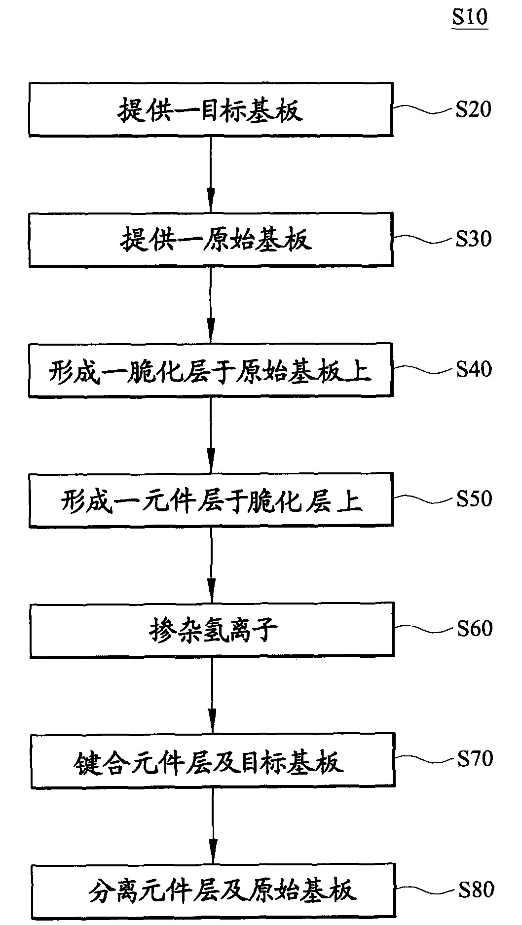
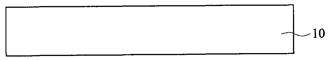
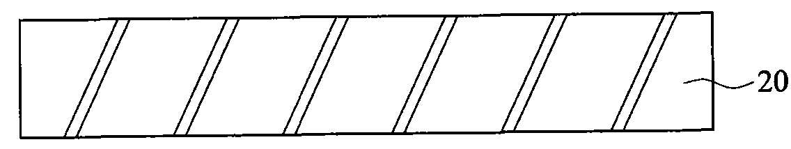
[0052] In order to further explain the technical means and effects that the present invention adopts to achieve the intended purpose of the invention, the method for manufacturing a substrate structure with a thin film formed by doping ions according to the present invention and its substrate will be described below in conjunction with the accompanying drawings and preferred embodiments. The specific implementation of the structure, manufacturing method, steps, structure, features and effects thereof are described in detail below.

[0053] The aforementioned and other technical contents, features and effects of the present invention will be clearly presented in the following detailed description of the preferred embodiments with reference to the drawings. Through the description of the specific implementation mode, a more in-depth and specific understanding of the technical means and effects adopted by the present invention to achieve the intended purpose can be obtained. Howev...


PUM


Abstract

This invention relates to a method for manufacturing a substrate structure which comprising a film and a substrate structure made by this method. The method for manufacturing a substrate structure comprising a film includes the steps of: providing a target substrate; providing an initial substrate; forming an embrittlement-layer on the initial substrate; forming a device layer on the embrittlement-layer; doping with hydrogen ions; bonding the device layer with the target substrate; and separating the device layer from the initial substrate. The hydrogen ions are added into the embrittlement-layer through doping, before an energy treatment is applied to embrittle and break the embrittlement-layer, thereby separating the device layer from the initial substrate. Since the hydrogen ions are added into the embrittlement-layer through doping, a crystal lattice structure of the device layer will not be damaged during the step of doping with hydrogen ions.

Description

technical field [0001] The invention relates to a method for manufacturing a substrate structure with a thin film and the substrate structure thereof, in particular to a method for manufacturing the substrate structure with a thin film by using doping ions and the substrate structure thereof. Background technique [0002] As disclosed in U.S. Patent No. 5,374,564, the method for manufacturing a thin film of semiconductor material is to implant high-dose ions such as gas ions such as hydrogen or inert gas into the original substrate to generate a gas ion layer, and then bond the original substrate to the target substrate. After being integrated, the gas ions are polymerized in the gas ion layer by heat treatment, and many microbubbles are generated. The microbubbles will gradually connect together, and then part of the original substrate will be separated up and down, and the separated original substrate will be transferred to the target substrate, thereby forming a thin film...

Claims


Application Information

Patent Timeline
Patent Type & Authority Applications(China)
IPC IPC(8): H01L21/00H01L21/18H01L21/20H01L21/762H01L21/84H01L23/00H01L27/12H01L27/01
CPCH01L21/76254
Inventor 李天锡赖朝松黄敬涵何嘉哲巫秉融郑守钧
Owner KINIK
Why Eureka
Try Eureka