Surface processing method for printed circuit board and corresponding printed circuit board

A printed circuit board and surface treatment technology, applied in the field of electronics, can solve the problems of increasing product cost, reduce the overall production cost and overcome the high cost effect

Active Publication Date: 2010-02-24
HUAWEI DEVICE CO LTD
View PDF0 Cites 5 Cited by
  • Summary
  • Abstract
  • Description
  • Claims
  • Application Information

AI Technical Summary

Problems solved by technology

However, for components that are not frequently plugged in, since the thickness of the gold layer in th

Method used


Image

  • Surface processing method for printed circuit board and corresponding printed circuit board
  • Surface processing method for printed circuit board and corresponding printed circuit board
  • Surface processing method for printed circuit board and corresponding printed circuit board

Examples


Embodiment Construction

[0015] The following will clearly and completely describe the technical solutions in the embodiments of the present invention with reference to the accompanying drawings in the embodiments of the present invention. Obviously, the described embodiments are only some, not all, embodiments of the present invention. Based on the embodiments of the present invention, all other embodiments obtained by persons of ordinary skill in the art without creative efforts fall within the protection scope of the present invention.

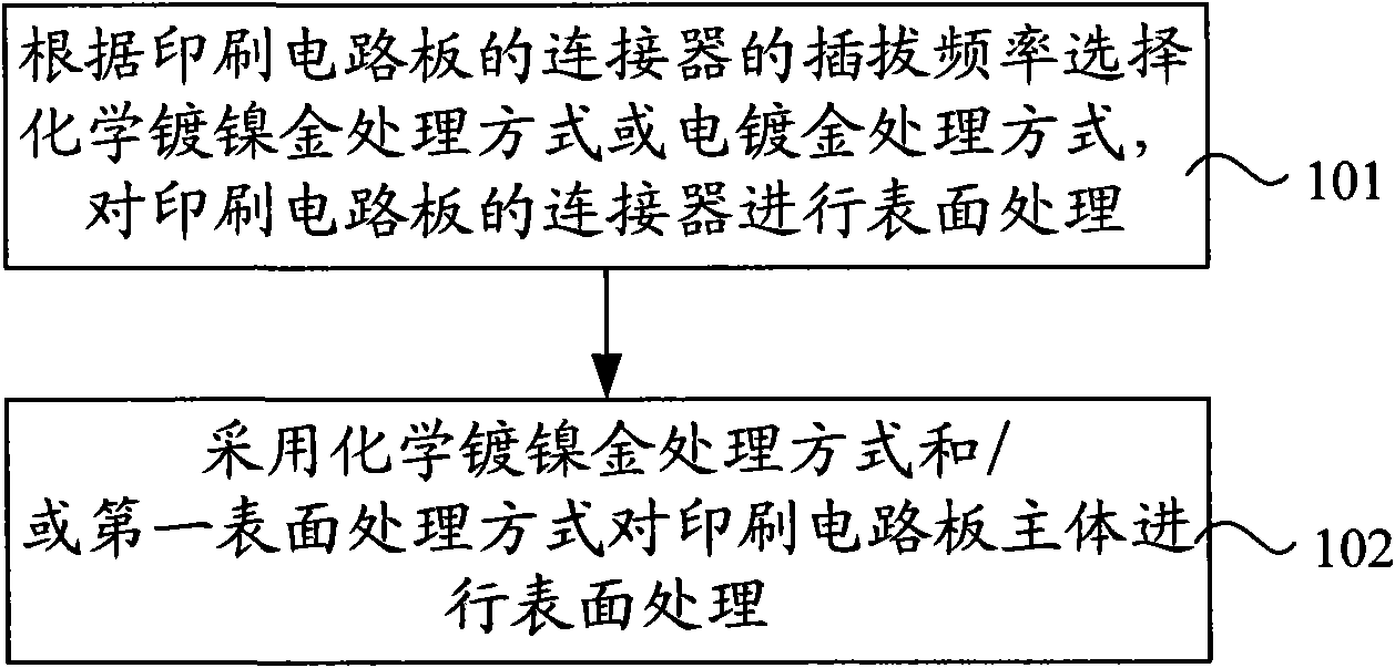
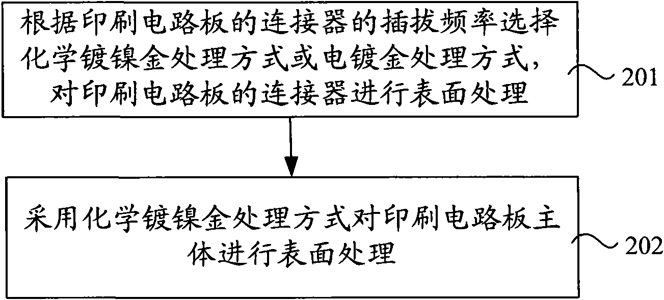
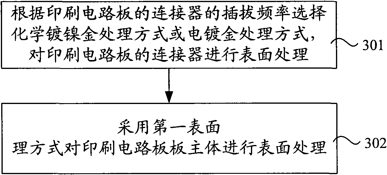
[0016] figure 1 It is a flowchart of an embodiment of the surface treatment method of a printed circuit board of the present invention, as figure 1 As shown, this embodiment provides a surface treatment method for a printed circuit board, which may specifically include the following steps:

[0017] In step 101 , the surface treatment of the connector of the printed circuit board is carried out by selecting an electroless nickel-plating treatment method or an elect...


PUM


Abstract

Embodiment of the invention discloses a surface processing method for a printed circuit board and the corresponding printed circuit board, wherein the surface processing method for a printed circuit board comprises selecting electroless nickel immersion gold processing mode or electrogilding processing mode according to plug frequency of connectors on the printed circuit board, performing surfaceprocessing on the connectors of the printed circuit board. The printed circuit board comprises a main body of PCB and the connectors, the surface processing mode of the connectors is electroless nickel immersion gold processing mode or electrogilding processing mode selected according to plug frequency of the connectors, and the surface processing mode of the main body of PCB is electroless nickelimmersion gold processing mode and/or a first surface processing mode. The invention differentiates the surface processing modes of the connectors of PCB with different plug frequencies, which reduces waste of resources.

Description

technical field [0001] The embodiments of the present invention relate to electronic technology, and in particular to a method for surface treatment of a printed circuit board and the printed circuit board. Background technique [0002] With the rapid development of telecommunications technology, various electronic products and components have emerged, and due to the increasingly fierce market competition, the structures and types of electronic products and components have become more and more diverse and complex. Among them, printed circuit boards (Printed Circuit Board; hereinafter referred to as: PCB) is used as a support for electronic components to provide electrical connections for various parts in electronic components. The interconnection between two PCBs is usually achieved through an edge connector commonly known as a gold finger, that is, inserting a gold finger on one PCB into a suitable slot on another PCB, such as a display card in a computer, The sound card, ...

Claims


Application Information

Patent Timeline
IPC IPC(8): H05K3/22H05K1/11
Inventor 景丰华赵龙敬勇
Owner HUAWEI DEVICE CO LTD
Why Eureka
Try Eureka