
Annealing treatment method for thinned or scribed gallium nitride base field-effect tube

A gallium nitride base field and annealing treatment technology, which is applied in the manufacture of electrical components, circuits, semiconductors/solid-state devices, etc., can solve problems such as device performance degradation, and achieve the effect of improving reliability and stabilizing characteristic parameters

Active Publication Date: 2012-04-18
INST OF MICROELECTRONICS CHINESE ACAD OF SCI
View PDF0 Cites 2 Cited by
  • Summary
  • Abstract
  • Description
  • Claims
  • Application Information

AI Technical Summary

Problems solved by technology

[0005] In view of the problem of device performance degradation after wafer thinning and slicing in the device manufacturing process, the present invention is proposed. For this reason, the main purpose of the present invention is to provide a method for annealing gallium nitride-based field effect transistors, to solve the above problems

Method used


Image

  • Annealing treatment method for thinned or scribed gallium nitride base field-effect tube
  • Annealing treatment method for thinned or scribed gallium nitride base field-effect tube
  • Annealing treatment method for thinned or scribed gallium nitride base field-effect tube

Examples


Embodiment Construction

[0014] Functional Overview

[0015] In an embodiment of the present invention, an annealing treatment scheme for GaN-based field effect transistors is provided. In this implementation scheme, slow annealing treatment is performed on GaN-based field effect transistors to improve thinning and scribing. The saturation leakage current of the GaN-based FET can be reduced, the leakage current when the FET is pinched off, and the DC performance and reliability of the GaN-based FET can be improved.

[0016] It should be noted that, in the case of no conflict, the embodiments in the present application and the features in the embodiments can be combined with each other. The present invention will be described in detail below with reference to the accompanying drawings and examples.

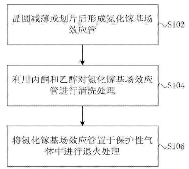
[0017] Such as figure 1 As shown, the present invention provides a method for annealing a GaN-based field effect transistor, comprising:

[0018] In step 102, the wafer is thinned and diced to form a ga...


PUM


Abstract

The invention provides an annealing treatment method for a thinned or scribed gallium nitride base field-effect tube, belonging to the technical field of a semiconductor. The method comprises the following steps: the thinned or scribed gallium nitride base field-effect tube is washed and treated by using acetone or alcohol; the washed and processed gallium nitride base field-effect tube is placedin protective gas for annealing treatment; the temperature for annealing treatment ranges from 200 to 400 DEG C; and the annealing time is of 30 to 60 hours. By the technical solution of the method, the long-standing slow annealing method used for treating the gallium nitride base field-effect tube can solve the problem that the direct current performance of the field-effect tube is degraded owing to the thinning and scribing, the increasing of the direct current performance of devices further increases the power performance of the devices, and characteristic parameters of the gallium nitridebase field-effect tube is stabilized after annealing, and further the reliability of the devices are increased.

Description

technical field [0001] The invention relates to the technical field of semiconductors, in particular to an annealing method for a thinned or sliced ​​GaN-based field effect transistor. Background technique [0002] In the manufacturing process of the semiconductor field effect transistor, the fabrication of the field effect transistor is completed after the thinning and scribing processes of the field effect transistor are performed. In the process of wafer thinning and dicing, it will inevitably be affected by mechanical stress, and the metal on the gate cap will affect the gate cap during AlGaN stress release due to the uneven stress distribution. The stress in the thin film will have a serious impact on the gate, thereby degrading the performance of the device. The formation of two-dimensional electron gas in GaN-based HEMT devices is mainly due to the polarization effect at the interface between AlGaN and GaN, which determines that the device is very sensitive to the in...

Claims


Application Information

Patent Timeline
Patent Type & Authority Patents(China)
IPC IPC(8): H01L21/335H01L21/324
Inventor 赵妙王鑫华刘新宇魏珂郑英奎
Owner INST OF MICROELECTRONICS CHINESE ACAD OF SCI
Learn More