Manufacturing method for multilayer stacking printed wiring board

A technology for printed circuit boards and production methods, which is applied in the direction of multi-layer circuit manufacturing, etc., can solve the problems of layer deviation scrapping, increase product production costs, complex process flow, etc., and achieve the effect of reducing production costs and improving product qualification rates.

Active Publication Date: 2010-03-03
DONGGUAN MEADVILLE CIRCUITS
View PDF0 Cites 15 Cited by
  • Summary
  • Abstract
  • Description
  • Claims
  • Application Information

AI Technical Summary

Problems solved by technology

[0003] The printed circuit board of the existing multi-layer stacked product (Sequential Lamination) is made by making two different sub-boards respectively, and then pressed together, and the process design is difficult (such as the minimum distance from the annular ring to the copper position (clearance) / hole-to-...

Method used


Image

  • Manufacturing method for multilayer stacking printed wiring board

Examples


Embodiment Construction

[0026] In order to further illustrate the technical means adopted by the present invention and its effects, the following describes in detail in conjunction with preferred embodiments of the present invention and accompanying drawings.

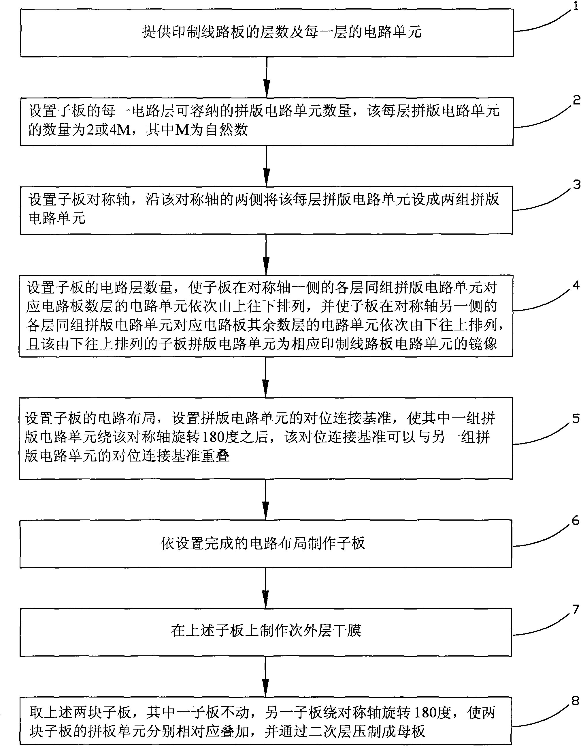
[0027] Such as figure 1 As shown, the manufacturing method of the multilayer superimposed printed circuit board of the present invention comprises the following steps:

[0028] Step 1, provide the number of layers of the printed circuit board and the circuit units of each layer.

[0029] Step 2, setting the number of imposition circuit units that can be accommodated in each circuit layer of the sub-board, the number of imposition circuit units in each layer is 2 or 4M, where M is a natural number.

[0030] Step 3, setting the symmetry axis of the sub-board, and setting the imposition circuit units of each layer into two groups of imposition circuit units along both sides of the symmetry axis.

[0031] Step 4: Set the number of circuit layers...


PUM


Abstract

The invention provides a manufacturing method for a multilayer stacking printed wiring board, comprising the steps of: (1) providing the number of layers of printed wiring board and a circuit unit ofeach layer, (2) setting the number of key-line layout circuit units which are contained in each circuit layer of a secondary board, (3) arranging a symmetry axis of the secondary board and disposing the key-line layout circuit units in each layer as two groups of key-line layout circuit units along the two sides of the symmetry axis, (4) setting the number of circuit layer of the secondary board,(5) distributing the circuit of the secondary board, (6) fabricating the secondary board according to the distributed circuit, (7) fabricating a secondary outer layer dry film on the secondary board,(8) taking two secondary boards, keeping one fixed and rotating the other for 180 DEG along the symmetry axis, respectively stacking the key-line layout units of the two secondary boards, and then fabricating a motherboard by secondary laminating. By adopting the design of male and female key-line layout, the invention can solve the problem of scrapping the products by avoiding the layer deflection caused by the swelling and contraction variance of the secondary board during secondary laminating, to promote the product percent of pass and decrease the manufacturing cost.

Description

technical field [0001] The invention relates to a method for manufacturing a multi-layer superimposed printed circuit board, in particular to a method for manufacturing a multi-layer superimposed printed circuit board using a yin-yang imposition design. Background technique [0002] In recent years, with the popularization of electronic products, the demand for printed circuit boards is also increasing. At the same time, with the miniaturization of electronic products, the requirements for high density of printed circuit boards are also increasing. Therefore, Existing printed circuit boards usually have a multi-layer structure and the circuits inside are becoming more and more dense. [0003] The printed circuit board of the existing multi-layer stacked product (Sequential Lamination) is made by making two different sub-boards respectively, and then pressed together, and the process design is difficult (such as the minimum distance from the annular ring to the copper positio...

Claims


Application Information

Patent Timeline
IPC IPC(8): H05K3/46
Inventor 梁敬业王建彬王佳
Owner DONGGUAN MEADVILLE CIRCUITS
Why Eureka
Try Eureka