TFT-LCD pixel structure, manufacturing method and broken wire repairing method

A pixel structure and pixel unit technology, which is applied in semiconductor/solid-state device manufacturing, nonlinear optics, optics, etc., can solve the problems of reduced maintenance success rate and long repair time

Active Publication Date: 2010-03-10
BOE TECH GRP CO LTD +1
View PDF0 Cites 56 Cited by
  • Summary
  • Abstract
  • Description
  • Claims
  • Application Information

AI Technical Summary

Problems solved by technology

However, it takes a long time to repair by chemical vapor deposition; if the area of ​​the fracture is large, the success rate of repair will be reduced

Method used


Image

  • TFT-LCD pixel structure, manufacturing method and broken wire repairing method
  • TFT-LCD pixel structure, manufacturing method and broken wire repairing method
  • TFT-LCD pixel structure, manufacturing method and broken wire repairing method

Examples


Embodiment Construction

[0035] The technical solutions of the present invention will be described in further detail below with reference to the accompanying drawings and embodiments.

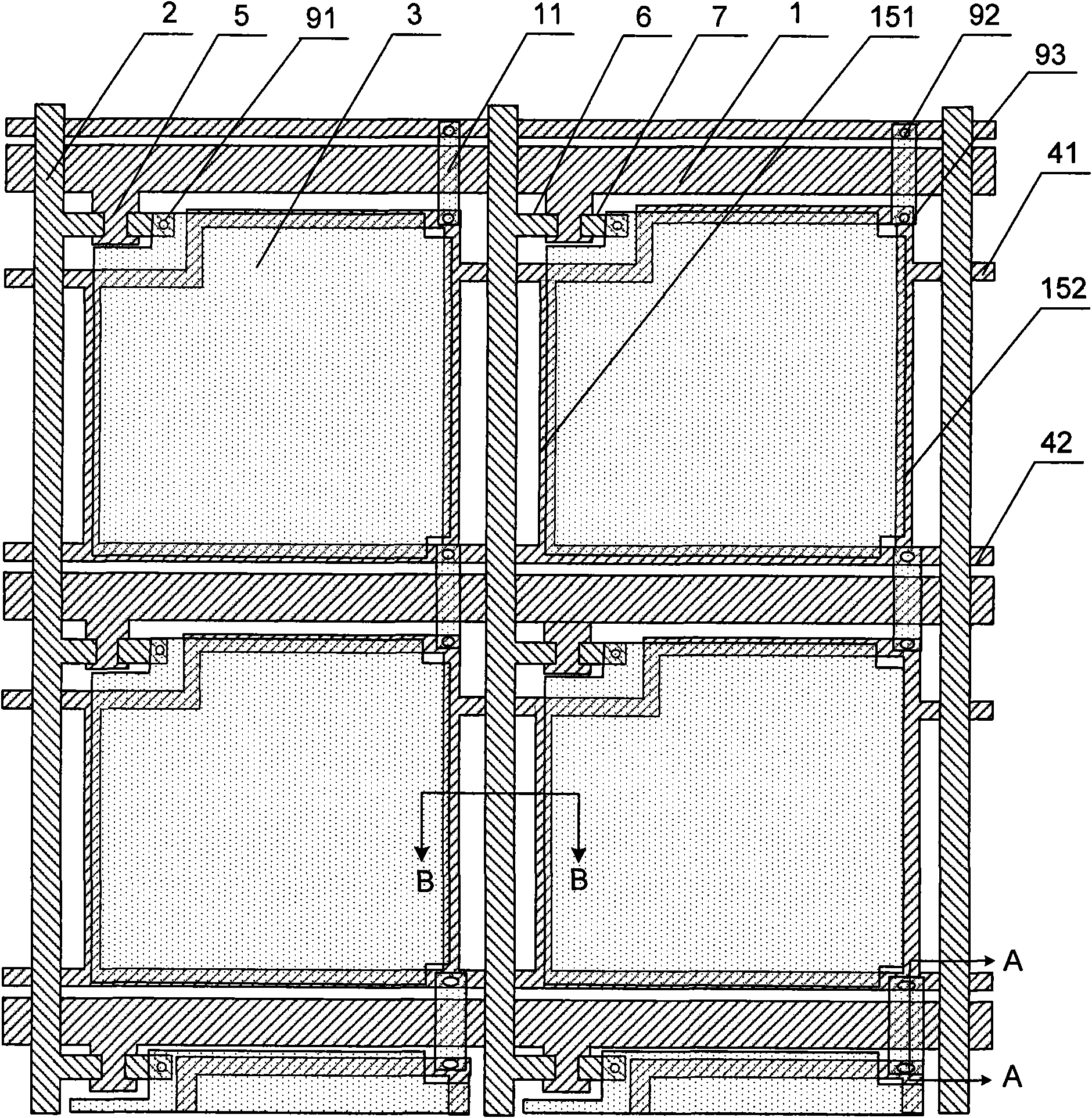
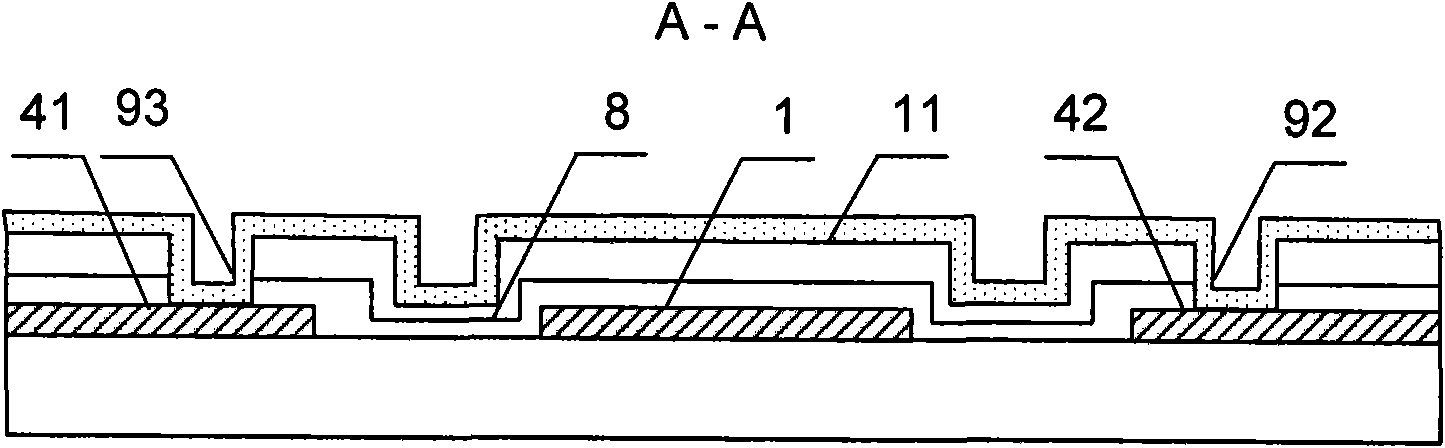
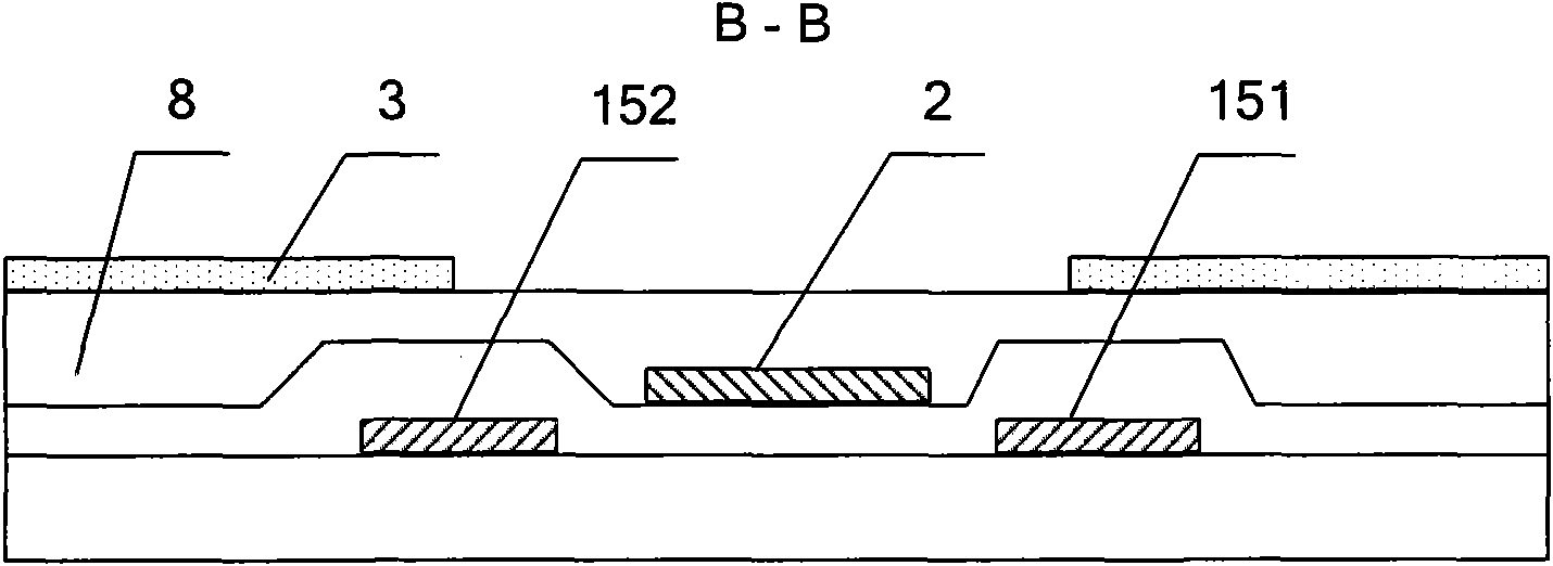
[0036] figure 1 It is a structural schematic diagram of a TFT-LCD pixel structure embodiment of the present invention, figure 2 for figure 1 Middle A-A sectional view, image 3 for figure 1 Middle B-B sectional view. Such as figure 1 , figure 2 and image 3As shown, the TFT-LCD pixel structure of this embodiment includes: gate lines 1, data lines 2, pixel electrodes 3, common electrode lines and thin film transistors (TFTs), and gate lines 1 and data lines 2 crossing each other define several pixels unit, and a thin film transistor is formed at the intersection, the pixel electrode 3 is formed in the pixel unit, and forms a storage capacitor with the common electrode line, which is a pixel structure in which the storage capacitor is on the common electrode line (Cst On Common). The thin film transistor struct...


PUM


Abstract

The invention relates to a TFT-LCD pixel structure, a manufacturing method and a broken wire repairing method. The TFT-LCD pixel structure comprises a plurality of pixel cells limited by a grid wire and a data wire, wherein a thin-film transistor and a pixel electrode are formed in each pixel cell, a first public electrode wire is formed on the lower side of the grid wire, a second public electrode wire is formed on the upper side of the grid wire, a first light blocking strip is formed on the left side of the pixel cell, and a second light blocking strip is formed on the right side of the pixel cell; the first public electrode wire, the second public electrode wire, the first light blocking strip and the second light blocking strip form an integrated structure and form an annular structure on the periphery of the pixel cell; and the second public electrode wire positioned on the upper side of the grid wire is connected with the first public electrode positioned on the lower side of the grid wire through a connecting electrode. The TFT-LCD pixel structure can be repaired quickly and efficiently, and has high success rate.

Description

technical field [0001] The invention relates to a liquid crystal display, in particular to a TFT-LCD pixel structure, a manufacturing method and a disconnection repairing method. Background technique [0002] Liquid Crystal Display (LCD) has the characteristics of small size, low power consumption, and no radiation, and has now occupied a dominant position in the field of flat panel display. The main structure of the liquid crystal display includes an array substrate and a color filter substrate that are boxed together and the liquid crystal is sandwiched between them. On the array substrate, gate lines that provide scanning signals, data lines that provide data signals, and pixel electrodes that form pixel points are formed. The manufacturing process of liquid crystal displays mainly includes the array process of preparing the array substrate and the color film substrate, the box forming process of combining the array substrate and the color film substrate and dripping the ...

Claims


Application Information

Patent Timeline
Patent Type & Authority Applications(China)
IPC IPC(8): G02F1/1362H01L27/12H01L21/84G02F1/13
Inventor 王峥
Owner BOE TECH GRP CO LTD
Why Eureka
Try Eureka