Organic light emitting display and method of manufacturing the same

a technology of organic light and display, which is applied in the direction of organic semiconductor devices, electrical devices, semiconductor devices, etc., can solve the problems of non-uniform picture quality and picture quality degradation, and achieve the effect of easy operation of manufacturing processes

Active Publication Date: 2012-08-16
SAMSUNG DISPLAY CO LTD
View PDF2 Cites 17 Cited by
  • Summary
  • Abstract
  • Description
  • Claims
  • Application Information

AI Technical Summary

Benefits of technology

[0009]It is another aspect of the present invention to provide a method of manufacturing an organic light emitting display in which auxiliary electrodes are coupled to cathode electrodes through contact regions generated by steps at a lower part of the auxiliary electrodes in order to facilitate manufacturing processes.
[0013]In the organic light emitting display according to the present invention, the auxiliary electrodes having the mesh structure are formed in the display region and the auxiliary electrodes are coupled to the cathode electrodes through the contact regions formed by the step parts in a lower part. The voltage of the cathode electrodes is uniformly maintained regardless of the positions of the pixels due to the auxiliary electrodes having the mesh structure so that a difference in brightness among the pixels is not generated. In addition, the auxiliary electrodes are coupled to the cathode electrodes through the contact regions formed by the step parts in the lower part so that manufacturing processes can be easily performed.

Problems solved by technology

However, since the transparent electrode material has a high resistivity, when the cathode electrodes are formed on the top of the display region in the form of a common electrode, a voltage difference between two locations at the common electrode occurs in accordance with the positions of the pixels corresponding to the two locations so that picture quality becomes non-uniform.
That is, since a difference in brightness occurs among the pixels due to a voltage difference (voltage drop) between the positions of the pixels close to an external power source and the positions of the pixels remote from the external power source, picture quality deteriorates.

Method used


Image

  • Organic light emitting display and method of manufacturing the same
  • Organic light emitting display and method of manufacturing the same
  • Organic light emitting display and method of manufacturing the same

Examples


first embodiment

[0025]FIGS. 1 and 2 are schematic drawings illustrating plan views of an organic light emitting display according to the present invention.

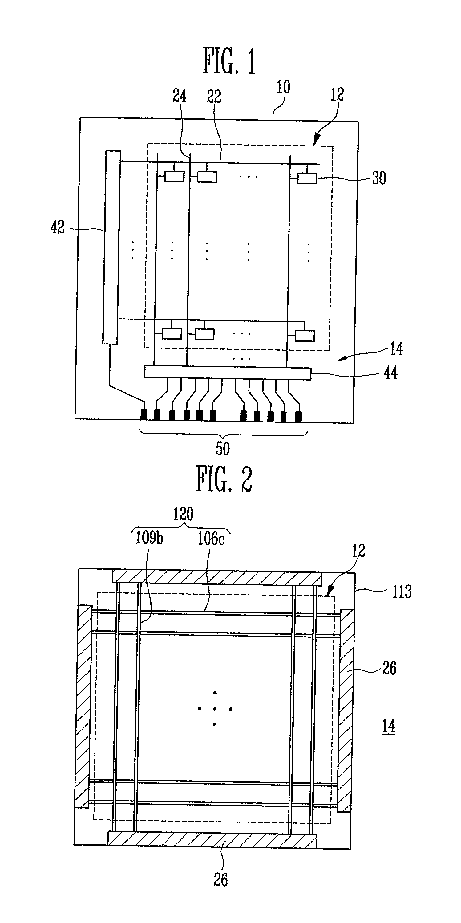
[0026]Referring to FIG. 1, a substrate 10 includes a display region 12 and a non-display region 14 around the display region 12. In the display region 12, a plurality of pixels 30 coupled to scan lines 22 and data lines 24 are arranged in a matrix. In the non-display region 14, drivers 42 and 44, which provide signals to the scan lines 22 and the data lines 24 respectively, and a pad unit 50, which receives signals from the outside, are provided.

[0027]The pixels 30 include anode electrodes, organic light emission layers, and cathode electrodes and can further include thin film transistors (TFT) that operate as switches.

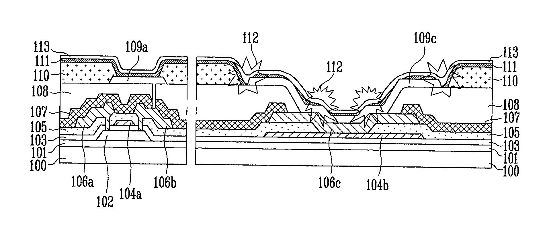
[0028]Referring to FIG. 2, a cathode electrode 113 is provided on the top of the display region 12 in the form of a common electrode. In addition, the cathode electrode 113 is coupled to auxiliary electrodes 120 provided under the ...

second embodiment

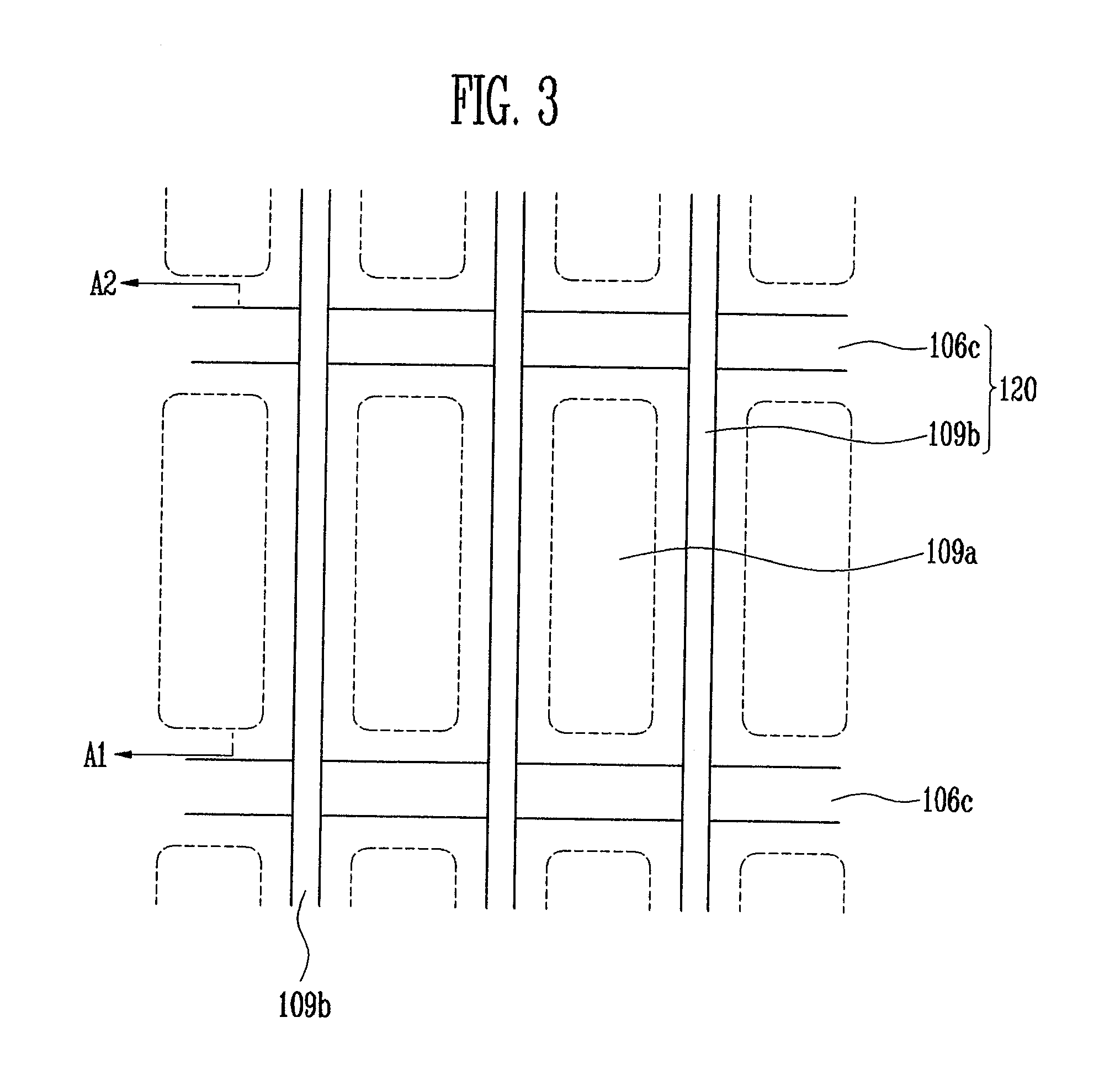
[0038]FIG. 6 is a plan view illustrating an organic light emitting display according to the present invention, which is an enlarged plan view of a portion of the display region 12 illustrated in FIG. 2. FIG. 7 is a sectional view taken along line B1-B2 of FIG. 6.

[0039]According to the first embodiment, the first auxiliary electrode 106c extending in one direction (X direction) is formed of the material of the source and drain electrodes 106a and 106b that constitute a thin film transistor (TFT). However, according to the second embodiment of the present invention, the auxiliary electrode extending in one direction (X direction) is formed to have a laminated structure, which includes the material of the source and drain electrodes 106a and 106b that constitute the TFT and the material of the anode electrode 109a that constitutes the pixel 30. Since a larger number of contact regions 112 are formed by the auxiliary electrodes having the laminated structure than those of the first embo...


PUM


Abstract

A top emission organic light emitting display and a method of manufacturing the same. The organic light emitting display includes a substrate, a plurality of thin film transistors (TFT) on the substrate, a plurality of first electrodes coupled to the plurality of TFTs, auxiliary electrodes having a mesh structure defining areas where the plurality of first electrodes are located, a pixel defining layer on a substantially entire area of the substrate and patterned to expose the first electrodes and the auxiliary electrodes, an organic light emission layer on the substantially entire area of the substrate including the exposed first electrodes and auxiliary electrodes, and second electrodes on the organic light emission layer. Steps are formed at lower parts of the auxiliary electrodes, and the second electrodes are coupled to the auxiliary electrodes through contact regions in which the auxiliary electrodes are exposed due to the steps.

Description

CROSS-REFERENCE TO RELATED APPLICATION[0001]This application is a divisional of U.S. patent application Ser. No. 12 / 566,653, filed Sep. 24, 2009, which claims priority to and the benefit of Korean Patent Application No. 10-2008-0118052, filed on Nov. 26, 2008, the entire content of both of which is incorporated herein by reference.BACKGROUND OF THE INVENTION[0002]1. Field of the Invention[0003]The present invention relates to a top emission organic light emitting display and a method of manufacturing the same.[0004]2. Description of the Related Art[0005]An organic light emitting display having a self-emission characteristic includes a substrate on which pixels are arranged, an encapsulating substrate arranged to face the substrate, and a sealant for sealing the pixels between the substrate and the encapsulating substrate.[0006]The organic light emitting display having the above structure is categorized as having a top emission structure or a bottom emission structure in accordance w...

Claims


Application Information

Patent Timeline
Patent Type & Authority Applications(United States)
IPC IPC(8): H01L33/62
CPCH01L27/3244H01L2251/5315H01L51/5234H10K2102/3026H10K59/131H10K59/80522H10K59/80524H10K59/122H10K50/828H10K50/824H10K59/12
Inventor BANG, HYUN-CHOLSUH, MI-SOOK
Owner SAMSUNG DISPLAY CO LTD
Why Eureka
Try Eureka